Semiconductor structure and manufacture method thereof

A manufacturing method and semiconductor technology, applied in the direction of semiconductor/solid-state device manufacturing, semiconductor devices, semiconductor/solid-state device components, etc., can solve the problems of semiconductor structure performance that need to be improved, so as to eliminate the problem of bonding offset and reduce adverse effects Effect

Active Publication Date: 2016-03-30
SEMICON MFG INT (SHANGHAI) CORP
View PDF3 Cites 9 Cited by
  • Summary
  • Abstract
  • Description
  • Claims
  • Application Information

AI Technical Summary

Problems solved by technology

[0006] However, the performance of the semiconductor structure formed

Method used


Image

  • Semiconductor structure and manufacture method thereof
  • Semiconductor structure and manufacture method thereof
  • Semiconductor structure and manufacture method thereof

Examples


Embodiment Construction

[0037] It can be seen from the background art that the performance of the semiconductor structure formed in the prior art needs to be improved.

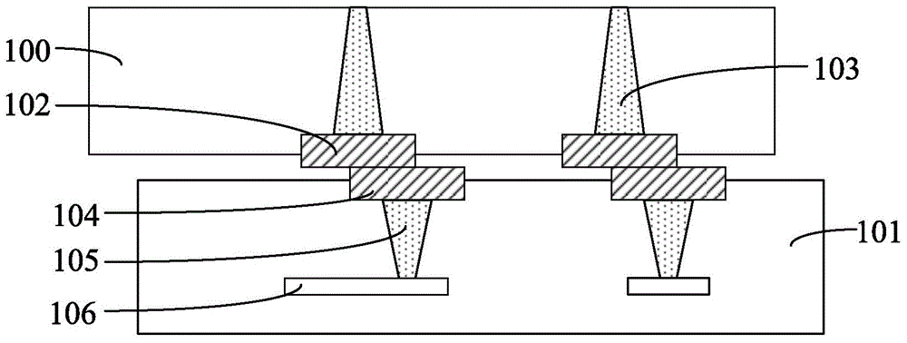
[0038] Please refer to figure 1 , in one embodiment, a first wafer 100 is provided, the first wafer 100 has a first plug 103 inside, and the first wafer 100 is also formed with a first plug electrically connected to the first plug 103. A metal layer 102, and the top of the first metal layer 102 is higher than the surface of the first wafer 100; a second wafer 101 is provided, and a second plug 105 is provided in the second wafer 101. A second metal layer 104 electrically connected to the second plug 105 is also formed in the circle 101 , and the top of the second metal layer 104 is higher than the surface of the second wafer 101 .

[0039] Please continue to refer figure 1 , performing an alignment process on the first wafer 100 and the second wafer 101, and then performing a bonding process on the first wafer 100 and the second wa...


PUM


Abstract

The present invention provides a semiconductor structure and a manufacture method thereof. The manufacture method of the semiconductor structure comprises: providing a first wafer and a second wafer, the first wafer being provided with a first metal layer, the second layer being provided with a second metal layer; forming a first material layer at the surface of the first wafer; forming a second material layer at the surface of the second wafer; performing alignment processing and bonding processing of the first wafer and the second wafer to align the first material layer with the second material layer and contact the surface of the first material layer with the surface of the second material layer; performing heat processing of the first material layer and the second material after the bonding processing to mutually fuse the first material layer and the second layer so that the alignment precision between the first metal layer and the second layer is improved. The surface tension generated by mutually fusing the first material layer and the second material layer is employed to get close the first material layer to the second material layer, so that the alignment precision between the first metal layer and the second layer is improved and the bonding offset is decreased.

Description

technical field [0001] The invention relates to the technology in the field of semiconductor manufacturing, in particular to a semiconductor structure and a manufacturing method thereof. Background technique [0002] With the rapid development of semiconductor manufacturing technology, in order to achieve faster computing speed, larger data storage capacity and more functions of semiconductor devices, semiconductor chips are developing towards higher integration. The higher the integration degree of the semiconductor chip, the smaller the characteristic size (CD: Critical Dimension) of the semiconductor device. [0003] A three-dimensional integrated circuit (3DIC: Three-Dimensional Integrated Circuit) is prepared by using advanced chip stacking technology, which is to stack chips with different functions into an integrated circuit with a three-dimensional structure. Compared with two-dimensional integrated circuits, the stacking technology of three-dimensional integrated c...

Claims


Application Information

Patent Timeline
IPC IPC(8): H01L23/48H01L23/52H01L21/60
CPCH01L2225/06513H01L2225/06541H01L2224/8113H01L24/05H01L24/11H01L24/13H01L24/16H01L24/81H01L24/94H01L2224/0401H01L2224/0557H01L2224/13007H01L2224/13023H01L2224/16146H01L2224/81132H01L2224/81143H01L2224/81193H01L2224/81203H01L2224/81815H01L2224/81986H01L2224/13006H01L25/0657H01L25/50H01L2225/06593H01L24/17H01L2224/17517H01L2224/10135H01L2224/81141H01L2224/05147H01L2224/05124H01L2224/05144H01L2224/05184H01L2224/05139H01L2224/05647H01L2224/05624H01L2224/05644H01L2224/05684H01L2224/05639H01L2224/05611H01L2224/05616H01L2224/05613H01L2224/13111H01L2224/13139H01L2224/13116H01L2224/13113H01L2224/1319H01L2224/0569H01L2224/05567H01L2224/81907H01L2224/81906H01L2224/8183H01L2224/8182H01L2924/00014H01L2924/013H01L2924/01047H01L2924/0105H01L2924/01082H01L2924/01083H01L2924/0665H01L2924/06H01L23/544H01L21/68H01L24/03H01L24/09H01L24/89H01L2224/03618H01L2224/05111H01L2224/05113H01L2224/05116H01L2224/08145H01L2224/8013H01L2224/80203H01L2224/80801H01L2924/0132H01L2924/0133H01L2924/20104H01L2924/20105H01L2924/20106H01L2924/20107H01L2924/20108H01L2924/20109
Inventor 丁敬秀何作鹏
Owner SEMICON MFG INT (SHANGHAI) CORP
Why Eureka
Try Eureka