Semiconductor device
A semiconductor and device technology, applied in the field of semiconductor devices, to achieve the effect of maintaining ESD resistance and promoting area reduction
- Summary
- Abstract
- Description
- Claims
- Application Information
AI Technical Summary
Benefits of technology
Problems solved by technology
Method used
Image
Examples
no. 1 example
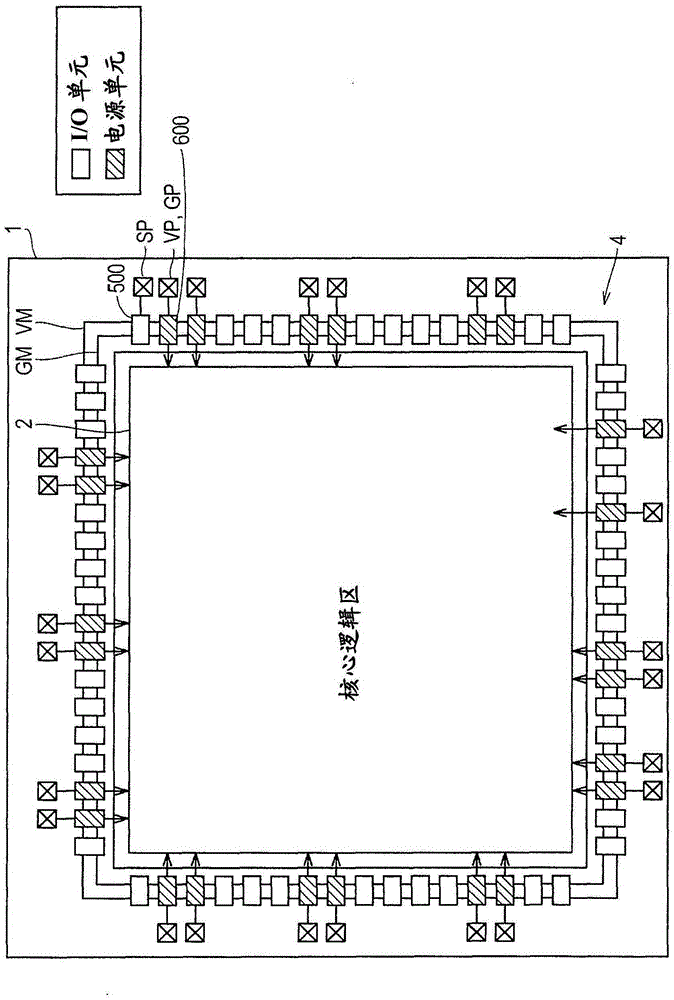
[0030] figure 1 is an explanatory diagram illustrating one example of the whole of the semiconductor device 1 according to the first embodiment.
[0031] Such as figure 1 Illustrated, semiconductor device 1 includes peripheral I / O area 4 provided in a peripheral area and core logic area 2 arranged in an inner area and configured as an ASIC (Application Specific Integrated Circuit) having a predetermined function.
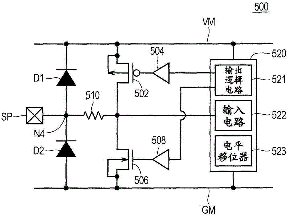
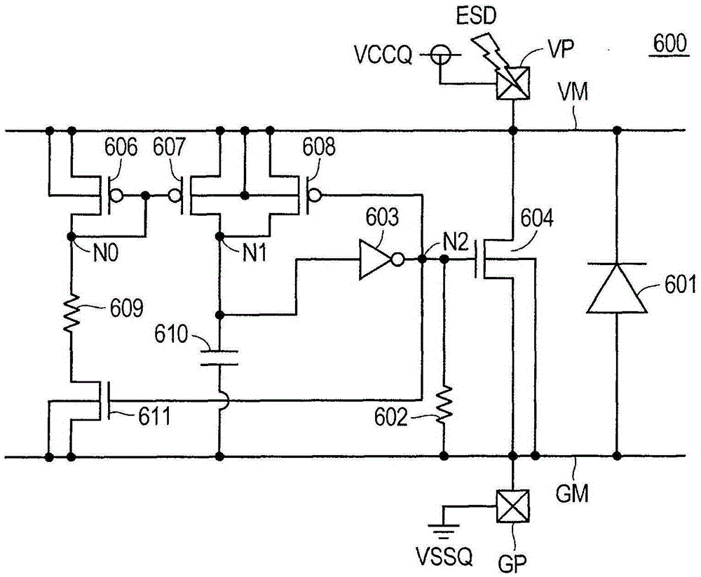
[0032] The peripheral I / O area 4 includes an I / O unit 500 serving as an input / output interface of signals, a power supply unit 600 receiving input from an external power supply, and the like. Here, exemplified is the case where the power line VM and the ground line GM are arranged in the peripheral area. A pad VP is a pad of a power supply and a pad GP is a pad of a ground, and the pad VP and the pad GP are coupled with the power supply unit 600 . The pad SP is a pad for signals and is coupled to the I / O cell 500 . Incidentally, pads VP, GP, SP along figure 1 T...
no. 2 example
[0105] In the second embodiment, a system configured to further improve ESD discharge characteristics will be described.
[0106] Figure 10A and Figure 10B are explanatory diagrams each illustrating one example of the circuit configuration of the power supply unit 600B according to the second embodiment. Figure 10A is an explanatory diagram of one example of the circuit configuration of the power supply unit 600B.
[0107] Such as Figure 10A As shown in , the power supply unit 600B differs from the power supply unit 600A in that an inverter 620 and a resistive element 621 have been further provided.
[0108] The inverter 620 outputs a signal to the node N3, and the node N1 serves as an input node. The gate of P-channel MOS transistor 608 is coupled to node N3. In addition, the N-channel MOS transistor 611 is coupled to the node N3.
[0109] The resistive element 621 is coupled between the node N3 and the ground line GM. The difference between the power supply unit 6...
no. 3 example
[0126] Figure 12A and Figure 12B are explanatory diagrams each illustrating one example of the circuit configuration of the power supply unit according to the third embodiment.
[0127] Figure 12A is an explanatory diagram illustrating one example of the circuit configuration of the power supply unit 700 . Such as Figure 12A As shown in , the power supply unit 700 differs from the power supply unit 600 in that the current mirror circuit is formed of N-channel MOS transistors.
[0128] Specifically, the power supply unit 700 differs from the power supply unit 600 in that N-channel MOS transistors 706, 707 and 708 have been provided to replace the P-channel MOS transistors 606, 607 and 608, and the P-channel MOS transistor 711 has been provided to replace N-channel MOS transistor 611, and an inverter 712 has also been added.
[0129] Specifically, N-channel MOS transistor 706 is coupled in series with resistive element 609 and P-channel MOS transistor 711 between power ...
PUM
 Abstract
Description
Claims
Application Information
 - R&D Engineer
- R&D Manager
- IP Professional
- Industry Leading Data Capabilities
- Powerful AI technology
- Patent DNA Extraction
Browse by: Latest US Patents, China's latest patents, Technical Efficacy Thesaurus, Application Domain, Technology Topic, Popular Technical Reports.
© 2024 PatSnap. All rights reserved.Legal|Privacy policy|Modern Slavery Act Transparency Statement|Sitemap|About US| Contact US: help@patsnap.com


