Cable and manufacturing method therefor, circuit protector and manufacturing method therefor, and load circuit
A circuit protection and load circuit technology, applied in resistor components, cable/conductor manufacturing, circuits, etc., can solve problems such as tight installation space, inability to install PTC circuit protection devices, and reduce cable layout density, to prevent excessive flow or overheating effect
- Summary
- Abstract
- Description
- Claims
- Application Information
AI Technical Summary
Problems solved by technology
Method used
Image
Examples
no. 1 example
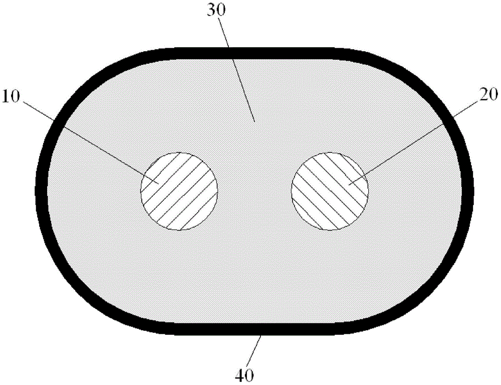
[0046] figure 1 shows a longitudinal sectional view of a cable according to a first embodiment of the present invention; figure 2 A transverse sectional view of a cable according to a first embodiment of the present invention is shown.
[0047] Such as figure 1 and figure 2 As shown, in one embodiment of the present invention, the cable mainly includes a first conductor 10 , a second conductor 20 and a PTC material layer 30 .
[0048] Such as figure 1 and figure 2 As shown, in the illustrated embodiment, the PTC material layer 30 is directly combined with the first conductor 10 and the second conductor 20 . The first conductor 10 and the second conductor 20 are spaced apart from each other and electrically connected to each other through the PTC material layer 30 .
[0049] In one embodiment of the present invention, there is also provided a method comprising figure 1 and figure 2 The load circuit of the cable shown is that the cable is connected in series on the l...
no. 2 example
[0063] image 3 shows a longitudinal sectional view of a cable according to a second embodiment of the present invention; Figure 4 A transverse sectional view of a cable according to a second embodiment of the present invention is shown.
[0064] Such as image 3 and Figure 4 As shown, in an embodiment of the present invention, the cable mainly includes a first conductor 100 , a second conductor 200 and a PTC material layer 300 .
[0065] Such as image 3 and Figure 4 As shown, in the illustrated embodiment, the PTC material layer 300 is directly combined with the first conductor 100 and the second conductor 200 . The first conductor 100 and the second conductor 200 are spaced apart from each other and electrically connected to each other through the PTC material layer 300 .
[0066] In one embodiment of the present invention, there is also provided a method comprising image 3 and Figure 4 The load circuit of the cable shown is that the cable is connected in serie...
PUM
 Abstract
Description
Claims
Application Information


