Array substrate, display panel and display device
A kind of technology of array substrate and base substrate
- Summary
- Abstract
- Description
- Claims
- Application Information
AI Technical Summary
Problems solved by technology
Method used
Image

Examples
Embodiment Construction
[0028] The specific implementation manners of the array substrate, the display panel and the display device provided by the embodiments of the present invention will be described in detail below with reference to the accompanying drawings.
[0029] Wherein, the size and shape of each structure in the drawings do not reflect the real proportion of the array substrate, and the purpose is only to illustrate the content of the present invention.
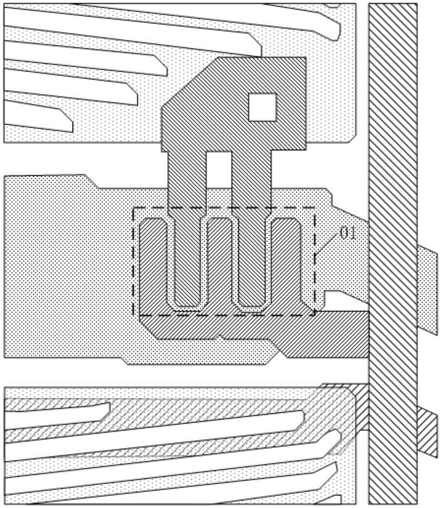
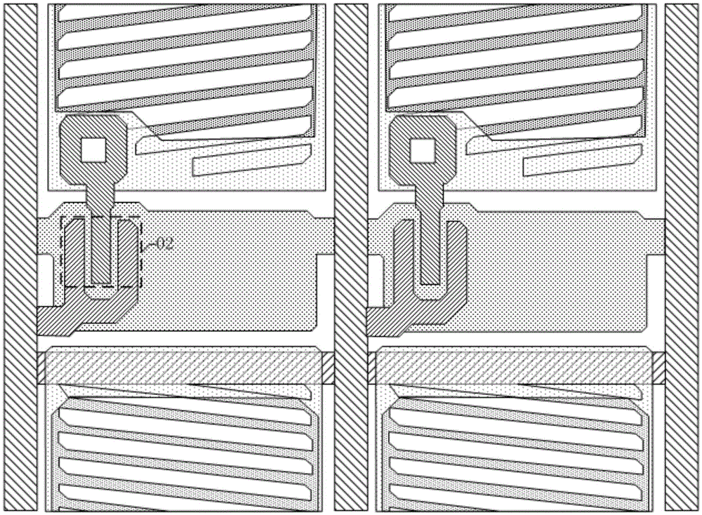
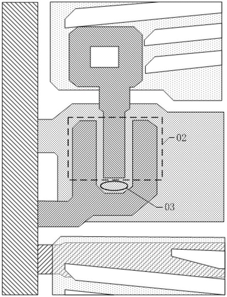
[0030] An embodiment of the present invention provides an array substrate, such as Figure 4 and Figure 5 As shown, it includes: a base substrate, a data line 1 and a thin film transistor arranged on the base substrate;
[0031] The source 2 of the thin film transistor includes a first sub-source 21 and a second sub-source 22; the first sub-source 21 and the second sub-source 22 are respectively connected to the data line 1;
[0032] The drain 3 of the thin film transistor includes a first sub-drain 31; the first sub-drain 31 is locat...
PUM
 Abstract
Description
Claims
Application Information
 - R&D Engineer
- R&D Manager
- IP Professional
- Industry Leading Data Capabilities
- Powerful AI technology
- Patent DNA Extraction
Browse by: Latest US Patents, China's latest patents, Technical Efficacy Thesaurus, Application Domain, Technology Topic.
© 2024 PatSnap. All rights reserved.Legal|Privacy policy|Modern Slavery Act Transparency Statement|Sitemap