Array substrate, display panel and preparation method of array substrate

A technology of array substrates and substrate substrates, which is applied in semiconductor/solid-state device manufacturing, electrical components, electric solid-state devices, etc., and can solve problems such as AMOLED yield decline

Active Publication Date: 2019-11-22
EVERDISPLAY OPTRONICS (SHANGHAI) CO LTD
View PDF4 Cites 9 Cited by
  • Summary
  • Abstract
  • Description
  • Claims
  • Application Information

AI Technical Summary

Problems solved by technology

[0004] The embodiment of the present application provides an array substrate, a display panel, and a method for preparing the array substrate, which are used to solve the problem of a short circuit between capacitors and power lines, signal lines, etc., resulting in a decrease in the yield of AMOLED.

Method used


Image

  • Array substrate, display panel and preparation method of array substrate
  • Array substrate, display panel and preparation method of array substrate
  • Array substrate, display panel and preparation method of array substrate

Examples


Embodiment Construction

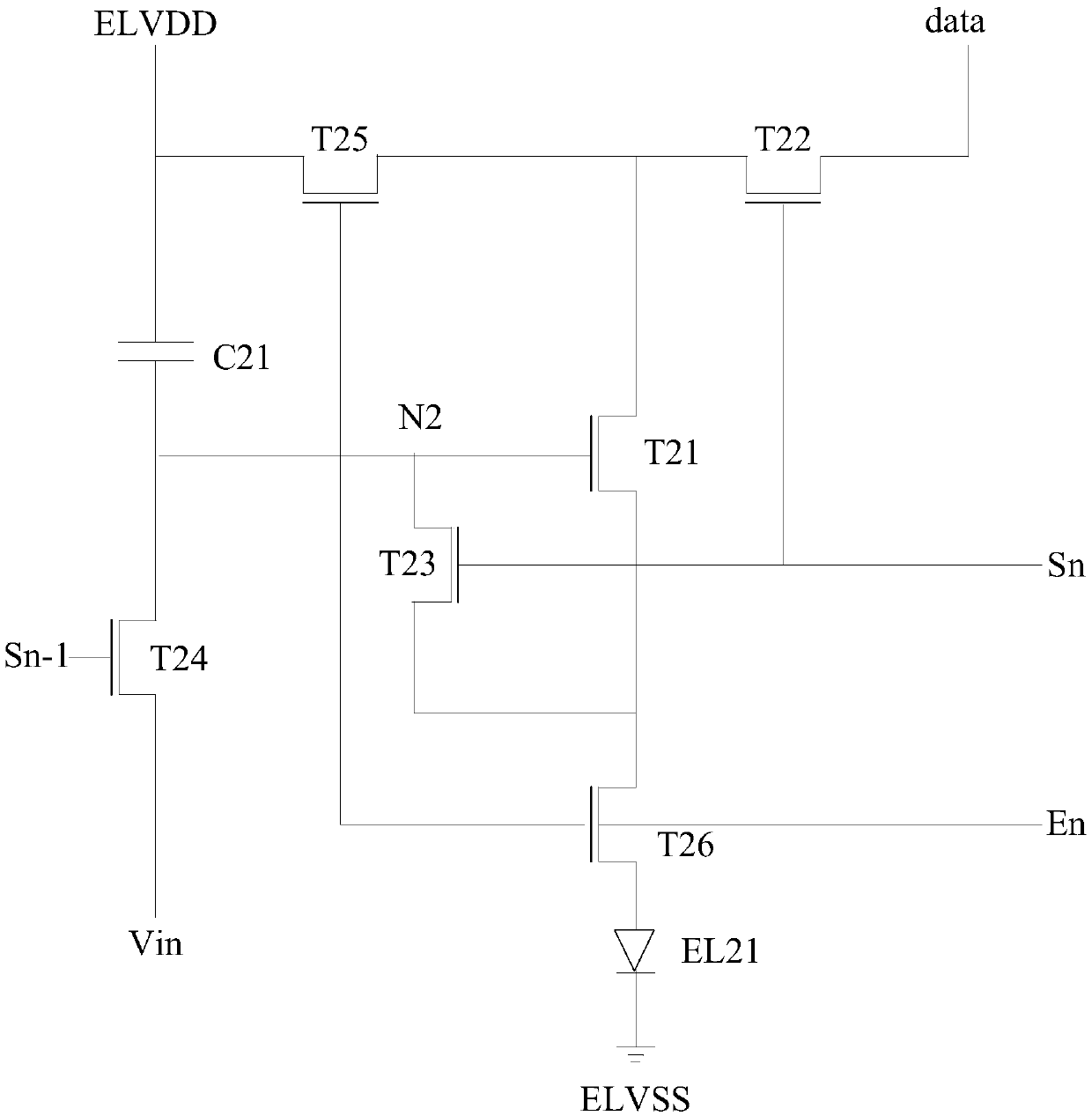
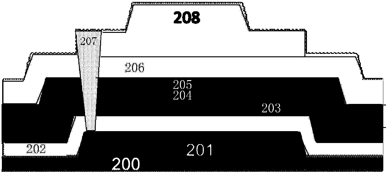
[0032] In the prior art, what AMOLED adopts is a thin film transistor (Thin Film Transistor, TFT) array, and polysilicon TFTs such as CMOS, PMOS, NMOS are prepared on the glass substrate first, and the light-emitting layer is prepared on the TFT, and the driving circuit is used to provide Controlled current to drive OLED, and continue to provide current after driving to ensure that each light-emitting pixel emits light continuously. The production process of AMOLED mainly includes: the production process of TFT and the production process of OLED; among them, the production process of TFT is mainly used to produce OLED drive circuit, TFT circuit is prepared on glass substrate; OLED production process is used to produce OLED pixels that emit light, which is mainly realized by evaporation.

[0033] TFT is divided into polysilicon and amorphous silicon. Among them, low temperature polysilicon (LTPS) is widely used due to its low temperature formation, large area, good space selecti...


PUM


Abstract

The invention discloses an array substrate, a display panel and a preparation method of the array substrate. The array substrate comprises a thin film transistor and a capacitor, and the capacitor comprises a first electrode layer, a first insulating layer and a second electrode layer which are arranged on a substrate; the orthographic projection area of the first electrode layer is a first area,and the orthographic projection area of the second electrode layer is a second area; an overlapping region of the orthographic projection regions of the first electrode layer, the first insulating layer and the second electrode layer forms a capacitor, the width of the second area is a first width, the width of the first area except the second area is a second width, and the first width is largerthan the second width.

Description

technical field [0001] The present application relates to the technical field of electronic displays, in particular to an array substrate, a display panel and a method for preparing the array substrate. Background technique [0002] Organic Light Emitting Diode (OLED for short) has the characteristic of self-illumination, adopts very thin organic material coating and substrate, when the current passes through, the organic material will emit light. The drive mode of OLED is divided into passive drive and active drive. Among them, active drive is active-matrix Organic Light Emitting Diode (AMOLED for short). Therefore, it has attracted much attention, and as a new generation display method, it is widely used in mobile phone screens, computer monitors, full-color computers, etc. [0003] AMOLED has become the mainstream of future display because of its advantages such as high color gamut and wide viewing angle. Due to the current technology and equipment of OLED products, it i...

Claims


Application Information

Patent Timeline
Patent Type & Authority Applications(China)
IPC IPC(8): H01L27/12H01L21/77H01L27/32
CPCH01L27/1214H01L27/1244H01L27/1259H01L2021/775H10K59/12
Inventor 劳浔
Owner EVERDISPLAY OPTRONICS (SHANGHAI) CO LTD
Why Eureka
Try Eureka