Display panel, manufacturing method of display panel and display device

A technology for display panels and manufacturing methods, applied in semiconductor/solid-state device manufacturing, instruments, electric solid-state devices, etc., can solve the problems of complex structure and high cost of display panels, and achieve the effects of reduced components, reduced thickness, and reduced process steps

Active Publication Date: 2016-04-13
SHANGHAI TIANMA MICRO ELECTRONICS CO LTD +1
View PDF4 Cites 22 Cited by
  • Summary
  • Abstract
  • Description
  • Claims
  • Application Information

AI Technical Summary

Problems solved by technology

[0004] Embodiments of the present invention provide a display panel, a manufacturing method thereof, and a display device, so as to solve the problems of complex structure and high cost of the display panel in the prior art

Method used


Image

  • Display panel, manufacturing method of display panel and display device
  • Display panel, manufacturing method of display panel and display device
  • Display panel, manufacturing method of display panel and display device

Examples


Embodiment Construction

[0023] In order to make the purpose, technical solutions and advantages of the present invention clearer, the technical solutions of the present invention will be clearly and completely described through implementation with reference to the accompanying drawings in the embodiments of the present invention. Obviously, the described embodiments are the embodiment of the present invention. Some, but not all, embodiments. Based on the embodiments of the present invention, all other embodiments obtained by persons of ordinary skill in the art without making creative efforts belong to the protection scope of the present invention.

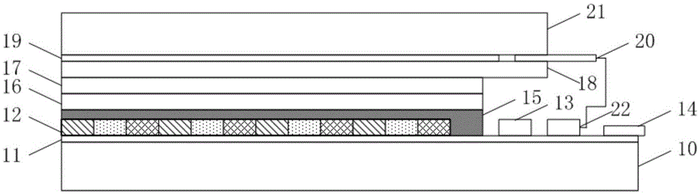
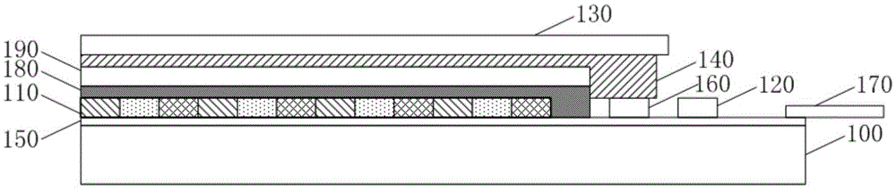
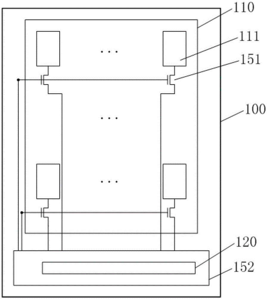
[0024] Such as Figure 2A Shown is a schematic diagram of a display panel provided by an embodiment of the present invention. The display panel provided in this embodiment includes: a substrate 100; an organic light-emitting layer 110 and a driving chip 120 disposed on the substrate 100, the organic light-emitting layer 110 is electrically connected to ...


PUM


Abstract

The embodiment of the invention discloses a display panel, a manufacturing method of the display panel and a display device. The display panel comprises a substrate, an organic light emitting layer arranged on the substrate, a driving chip arranged on the substrate, a protecting film and a touch electrode layer, wherein the organic light emitting layer is electrically connected with the driving chip, the protecting film is arranged on the side, far away from the substrate, of the organic light emitting layer, the touch electrode layer is arranged on the surface of the side, facing the organic light emitting layer, of the protecting film, and the touch electrode layer extends to the periphery of the organic light emitting layer and is electrically connected with the driving chip. According to the display panel, the touch electrode layer and the organic light emitting layer of the display panel share the driving chip; compared with the prior art, the structure of the display panel is simple, assemblies are reduced, corresponding cost and corresponding technological steps are reduced, the thickness of the display panel is also correspondingly reduced, and thinning and light weight of the display panel are achieved.

Description

technical field [0001] Embodiments of the present invention relate to display technologies, and in particular, to a display panel, a manufacturing method thereof, and a display device. Background technique [0002] At present, the touch module of the organic light emitting display panel is mainly made by processes such as on-cell touch (On-CellTouch), flexible touch (FilmTouch) or full bonding (OGS). figure 1 A schematic diagram of an organic light emitting display panel provided in the prior art. Such as figure 1 As shown, the display panel includes a substrate 10, a thin film transistor array 11, an organic light-emitting layer 12, a display driver chip 13, a first flexible circuit board 14, an encapsulation layer 15, a first adhesive material 16, a protective layer 17, and a touch electrode layer 18. A second adhesive material 19 , a second flexible circuit board 20 , a cover plate 21 and a touch driver chip 22 . Wherein, the touch electrode layer 18 is electrically co...

Claims


Application Information

Patent Timeline
Patent Type & Authority Applications(China)
IPC IPC(8): H01L27/32H01L51/52H01L51/56G06F3/041
CPCG06F3/0412G06F2203/04103H10K59/40H10K50/844H10K71/00
Inventor 霍思涛
Owner SHANGHAI TIANMA MICRO ELECTRONICS CO LTD
Why Eureka
Try Eureka