Circuit board testing apparatus and circuit board testing method

A substrate inspection and substrate technology, which is applied in measurement devices, electronic circuit testing, instruments, etc., can solve problems such as errors, and achieve excellent accuracy, reliability and easy confirmation.

Active Publication Date: 2016-04-20
NIDEC-READ CORPORATION
View PDF5 Cites 4 Cited by
  • Summary
  • Abstract
  • Description
  • Claims
  • Application Information

AI Technical Summary

Problems solved by technology

[0012] In addition, in the technology disclosed in Patent Document 1, when two contacts are short-circuited, a closed circuit is formed even if they are not in contact with the inspection point, and it is wrongly determined that the contacts are in contact with the inspection point. point

Method used


Image

  • Circuit board testing apparatus and circuit board testing method
  • Circuit board testing apparatus and circuit board testing method
  • Circuit board testing apparatus and circuit board testing method

Examples


Embodiment Construction

[0049] The best mode for carrying out the present invention will be described.

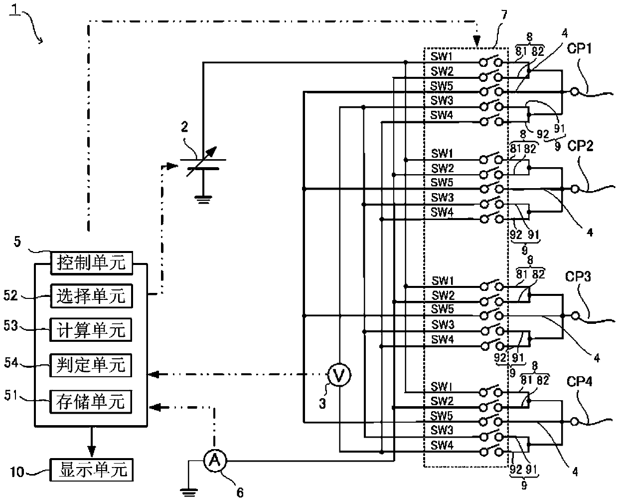
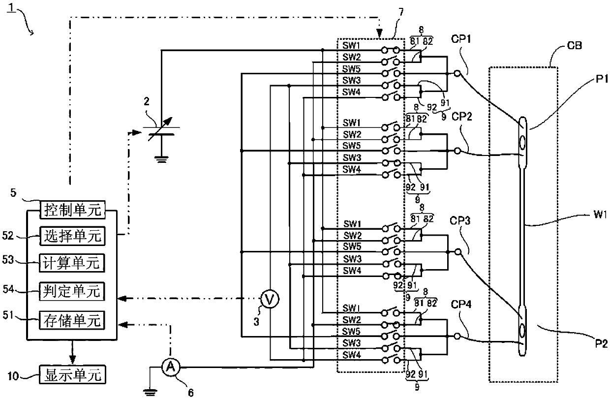
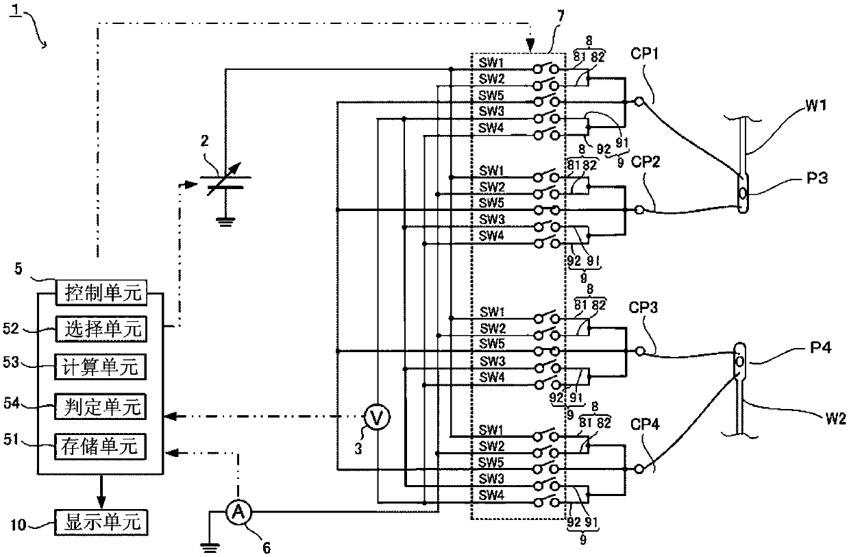
[0050] figure 1 It is a schematic structural diagram of the board|substrate inspection apparatus of this invention.

[0051] The substrate inspection device 1 of the present invention has a power supply unit 2, a detection unit 3, a connection terminal 4, a control unit 5, a storage unit 51, a selection unit 52, a calculation unit 53, a determination unit 54, a current detection unit 6, a switching unit 7, a power Terminal 8, detection terminal 9 and display unit 10.

[0052] In this substrate inspection apparatus 1 , contacts (contact probes) CP are used in order to make conductive contact with inspection points set on a plurality of wirings (between inspection points) Rx formed on the substrate. Through this contact CP, a predetermined potential and / or current can be applied to a predetermined inspection point, or an electrical characteristic (electrical signal) can be detected from a predeter...


PUM


Abstract

The invention relates to a circuit board testing method capable of simply and conveniently confirming abutting connection between contacts and a checking point in short time and a circuit board testing apparatus. The method is a four-terminal measurement method on a wiring pattern formed of a plurality of wires on a circuit board. The method and the apparatus are characterized in that an upstream-side detecting terminal connected to a detecting unit is in series connection with a contact of a downstream-side detecting terminal, electric power is supplied to the contacts in series connection to perform electric measurement between the contacts in series connection, electric characteristic of the contacts in series connection can be calculated according to electricity and electric measurement results, and the on-off state between the contacts in series connection and the checking point is determined based on the calculated electric characteristics.

Description

technical field [0001] The present invention relates to a substrate inspection method and a substrate inspection device for inspecting a substrate, and more specifically, to a substrate inspection method and a substrate inspection device in which a contact provided on an inspection jig is brought into contact with a contact set on a substrate. When the inspection is performed at the inspection point, it is possible to easily confirm that the contacts are in contact with the inspection point in a short time. [0002] It should be noted that the present invention is not limited to printed wiring boards, for example, can be applied to flexible substrates, multilayer wiring boards, electrode plates for liquid crystal displays and / or plasma displays, electrode plates for touch panels, and packaging for semiconductor packaging. Inspection of electrical wiring formed on various substrates such as substrates and / or film carriers and / or semiconductor wafers, etc., these various inspect...

Claims


Application Information

Patent Timeline
Patent Type & Authority Applications(China)
IPC IPC(8): G01R31/28G01R31/02G01R27/14
CPCG01R31/2812G01R31/54
Inventor 山下宗宽
Owner NIDEC-READ CORPORATION
Why Eureka
Try Eureka