Unit figure of LED photonic crystal structure and use method thereof

A photonic crystal and pattern technology, applied in the field of integrated circuit equipment manufacturing, can solve the problems of low luminous efficiency and no directionality, and achieve the effect of optimizing the photolithography process and meeting the large size

Active Publication Date: 2016-04-20
SHANGHAI MICRO ELECTRONICS EQUIP (GRP) CO LTD
View PDF3 Cites 1 Cited by
  • Summary
  • Abstract
  • Description
  • Claims
  • Application Information

AI Technical Summary

Problems solved by technology

[0002] Traditional light-emitting diodes (LEDs) have no directional light emission, so their luminous efficiency is not high in application. With the continuous development of LED manufacturing technology, photonic crystal technology has been introduced into the production of LED chips, which greatly improves the light extraction rate. At present, LED photonic crystal technology has become the most promising technology

Method used


Image

  • Unit figure of LED photonic crystal structure and use method thereof
  • Unit figure of LED photonic crystal structure and use method thereof
  • Unit figure of LED photonic crystal structure and use method thereof

Examples


Embodiment Construction

[0051] Specific embodiments of the present invention will be described in detail below in conjunction with the accompanying drawings.

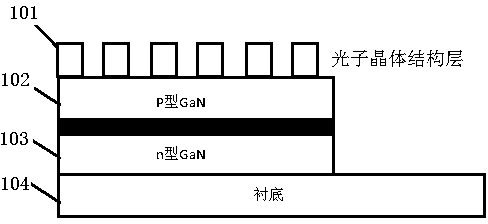
[0052] The process sequence of the LED photonic crystal process layer in the prior art is divided into four steps, including making the LED chip substrate, depositing the photonic crystal process layer, forming the photonic crystal structure by photolithography, and forming the photonic crystal pattern process layer by etching. The technical scheme of the invention is mainly applied to the photolithography process of the photonic crystal structure layer.

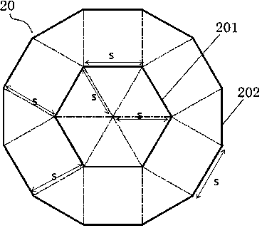
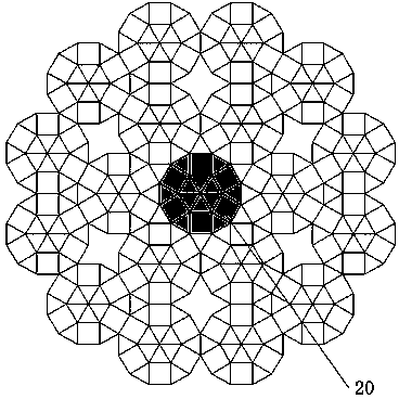
[0053] The lithography process of the photonic crystal structure layer specifically includes: first, glue is applied on the LED substrate sheet with the photonic crystal process layer; The mask plate operation of the pattern, with which the pattern is spliced ​​and exposed according to the stepping or scanning in the X and Y directions; after exposure, the final lithography photonic crystal ...


PUM


Abstract

The invention discloses a lithography splicing method of a photonic crystal process layer. The method is characterized by including: step 1. defining a photonic crystal structure figure characteristic, which refers to a figure structure with a spacing to the figure center of s, a regular hexagon inner ring and a regular dodecagon outer ring, wherein the s is two times larger than that of projection mask aligner minimum resolution R; step 2. forming a photonic crystal structure according to the photonic crystal structure figure characteristic; step 3. extracting a hexagon structure from the photonic crystal structure to serve as the unit figure; and step 4. taking a mask image containing the unit figure as the exposure field exposure field of view. The invention also discloses a mask containing the unit figure of the photonic crystal structure, a making method of the photonic crystal process layer, and a making method of the mask containing the unit figure of the photonic crystal structure.

Description

technical field [0001] The invention relates to the field of integrated circuit equipment manufacturing, in particular to a photonic splicing method for a unit pattern of an LED photonic crystal structure, a mask plate containing the pattern, and an LED photonic crystal process layer. Background technique [0002] Traditional light-emitting diodes (LEDs) have no directional light emission, so their luminous efficiency is not high in application. With the continuous development of LED manufacturing technology, photonic crystal technology has been introduced into the production of LED chips, which greatly improves the light extraction rate. At present, LED photonic crystal technology has become the most promising technology. [0003] A photonic crystal is a periodic structure that can interact with light. The behavior of light can be controlled by using the arrangement period, spatial structure and dielectric constant of the medium. When the frequency of light emitted by the ...

Claims


Application Information

Patent Timeline
Patent Type & Authority Applications(China)
IPC IPC(8): G03F1/00G03F7/20
Inventor 张家锦章磊熊威
Owner SHANGHAI MICRO ELECTRONICS EQUIP (GRP) CO LTD
Why Eureka
Try Eureka