Supercharge Your Innovation With Domain-Expert AI Agents!

Manufacturing method of input device

A manufacturing method and technology of an input device, which are applied in the input/output process of data processing, instruments, electrical digital data processing, etc., can solve the problems of not becoming wiring resistance, low wiring pattern adhesion, and increased wiring resistance. , to achieve full electrical connection reliability, narrow wiring, and low wiring resistance.

Inactive Publication Date: 2016-04-20
ALPS ALPINE CO LTD
View PDF4 Cites 1 Cited by
  • Summary
  • Abstract
  • Description
  • Claims
  • Application Information

AI Technical Summary

Problems solved by technology

[0011] However, since the wiring width is reduced, there is a problem that the wiring resistance becomes high and the detection responsiveness decreases.
In Patent Document 1, at the position of the contact hole, a wiring pattern with a substantially constant thickness is formed following the sidewall of the contact hole, but it does not have a structure capable of suppressing an increase in wiring resistance.
In addition, a thinner wiring pattern has lower adhesion and lower electrical connection reliability
[0012] In addition, when an insulating layer having a contact hole is formed by screen printing, the film thickness becomes relatively thick, and since the depth of the contact hole is deep, there is a possibility that the electrical connection between the upper and lower wiring layers cannot be properly connected through the contact hole. connection problem
Furthermore, in a structure in which the wiring layer is formed by Ag screen printing or the like as in the prior art, there is also a problem that the wiring layer cannot be formed at a narrow pitch.

Method used


Image

  • Manufacturing method of input device
  • Manufacturing method of input device
  • Manufacturing method of input device

Examples


Embodiment Construction

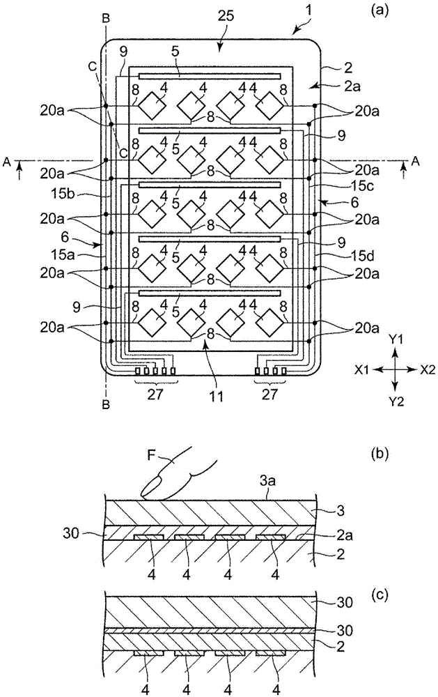
[0053] figure 1 (a) is a plan view of the input device (touch panel) in this embodiment, figure 1 (b) is to figure 1 (a) a partial longitudinal sectional view taken along the line A-A and viewed from the direction of the arrow, figure 1 (c) is with figure 1 (b) Partial longitudinal sectional view of a different embodiment.

[0054] In addition, in this specification, "transparency" and "transparency" refer to the state in which the visible light transmittance is 50% or more (preferably 80% or more). Furthermore, a haze value of 6 or less is optimal.

[0055] It should be noted that, in figure 1 In the figure, the respective transparent electrodes 4, 5 and the wiring portion 6 formed on the surface (first surface) 2a of the transparent substrate 2 constituting the input device 1 are shown, but the actual figure 1 As in (b), since the transparent panel 3 is provided on the front side of the transparent substrate 2 and the decorative layer exists at the position of the wiri...


PUM


Abstract

The object of the present invention is to provide an input device, which suppresses the increase of wiring resistance as compared with the prior art. The input device includes: a transparent substrate (2); a first wiring layer (8), which is formed by extending from each transparent electrode (3) to a decorative region (25) on a side of a display area; an insulating layer (20), which has a contact hole (20a) at a position opposite to a surface of the first wiring layer (8) and is formed on the surface side of the transparent substrate; a conductive portion (21), which is formed in the contact hole (20a); and a second wiring layer (15a), which is integrally formed with the conductive portion (21) and extends to the surface of the insulating layer (20) and is electrically connected to the first wiring layer (8 ). A side wall surface (20c) of the contact hole (20a) is gradually increased from the width T1 of the contact hole (20a) to form an inclination surface from the surface of the first layer toward the surface of the insulating layer. Moreover, the conductive portion (21) is filled inside the contact hole.

Description

[0001] This application is a divisional application of an invention patent application with an application date of December 27, 2012, an application number of 2012105797340, and an invention title of "input device and its manufacturing method". technical field [0002] The present invention relates to an input device capable of detecting the operation position of an operation surface, and in particular to a structure of a wiring layer arranged in a decoration area. Background technique [0003] In a capacitive input device (touch panel), a plurality of transparent electrodes are arranged in a display area of ​​a transparent substrate, and each first wiring layer drawn from each transparent electrode extends to a decoration area around the display area. . [0004] In Patent Document 1 figure 1 C. figure 2 B. In FIG. 5, a second wiring layer different from the first wiring layer is provided, and the first wiring layer and the second wiring layer are electrically connected t...

Claims


Application Information

Patent Timeline
Patent Type & Authority Applications(China)
IPC IPC(8): G06F3/041G06F3/044
CPCG06F3/041G06F3/044G06F2203/04103G06F3/0416
Inventor 佐藤清竹内正宜青木大悟
Owner ALPS ALPINE CO LTD
Features
  • R&D
  • Intellectual Property
  • Life Sciences
  • Materials
  • Tech Scout
  • Unparalleled Data Quality
  • Higher Quality Content
  • 60% Fewer Hallucinations
Learn More