Supercharge Your Innovation With Domain-Expert AI Agents!

Semiconductor storage device, and method for reading stored data

A storage device and semiconductor technology, which is applied in the direction of information storage, static memory, read-only memory, etc., and can solve problems such as the deterioration of the reading characteristics of the sense amplifier

Active Publication Date: 2016-04-20
키오시아가부시키가이샤
View PDF6 Cites 2 Cited by
  • Summary
  • Abstract
  • Description
  • Claims
  • Application Information

AI Technical Summary

Problems solved by technology

Therefore, it becomes the main cause of the deterioration of the read characteristic of the sense amplifier

Method used


Image

  • Semiconductor storage device, and method for reading stored data
  • Semiconductor storage device, and method for reading stored data
  • Semiconductor storage device, and method for reading stored data

Examples


Embodiment Construction

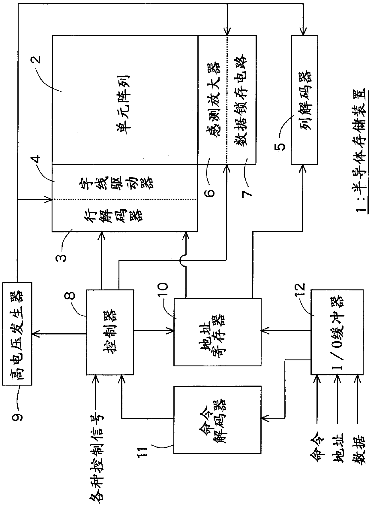
[0035] figure 1 It is a block diagram showing a schematic configuration of a semiconductor memory device according to an embodiment of the present invention. figure 1 The semiconductor memory device of 2009 shows an example of a NAND-type flash memory.

[0036] figure 1 The semiconductor storage device 1 includes: a cell array 2, a row decoder 3, a word line driver 4, a column decoder 5, a sense amplifier (S / A) 6, a data latch circuit 7, a controller 8, a high voltage generator 9. Address register 10, command decoder 11, I / O buffer 12.

[0037] The cell array 2 includes NAND strings in which a plurality of memory cells are connected in series.

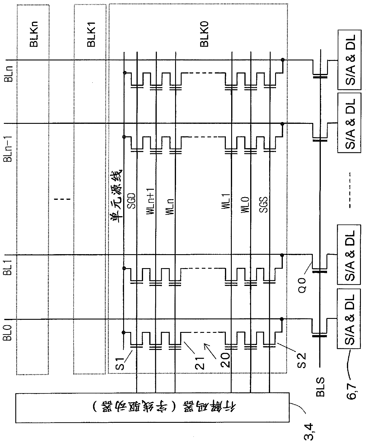
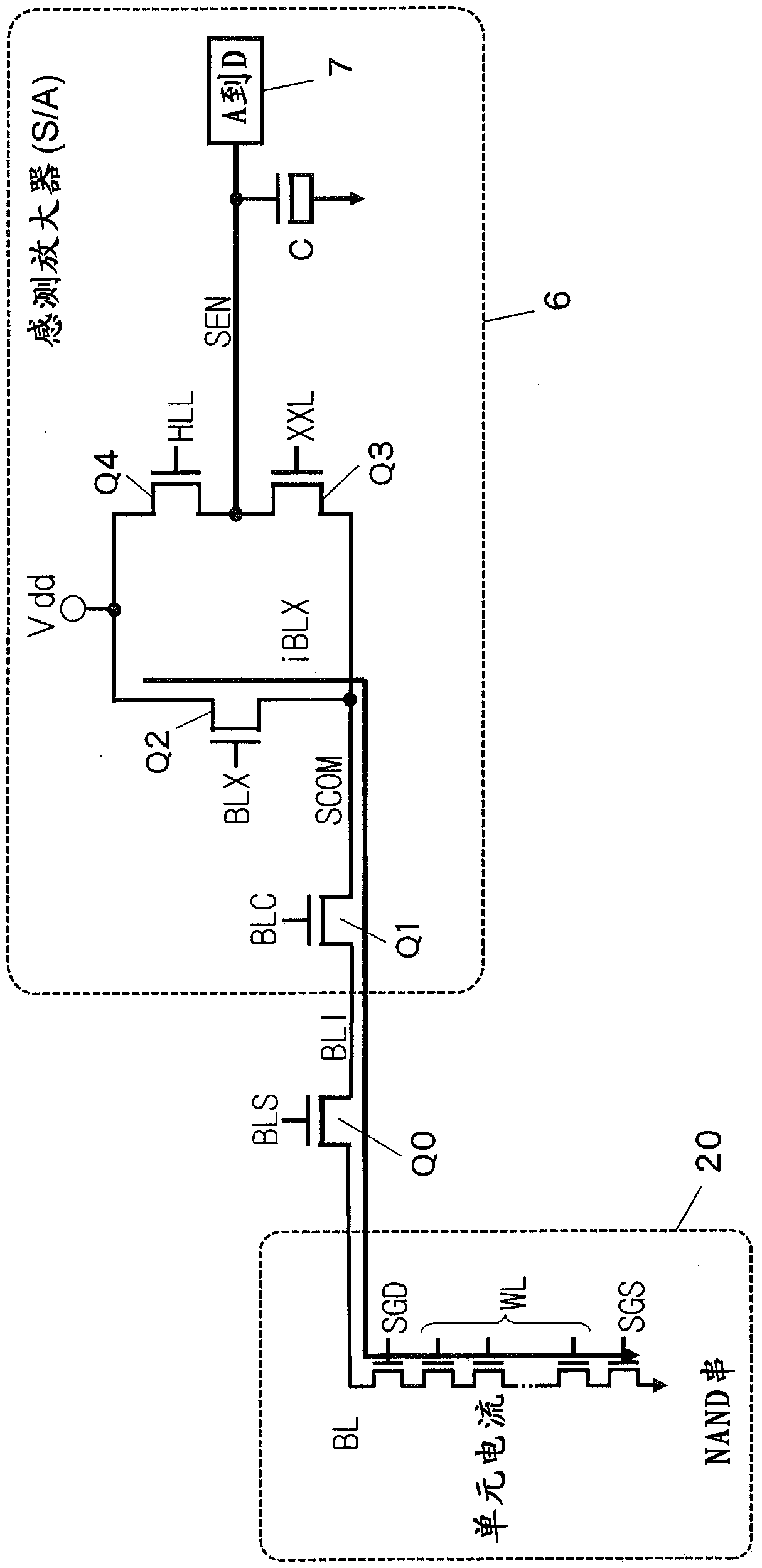
[0038] figure 2 It is a block diagram showing the detailed configuration around the cell array 2 . Such as figure 2 As shown, the cell array 2 is divided into a plurality of blocks BLK0˜BLKn. In each block, a plurality of the above-mentioned NAND strings 20 are arranged in the column direction. Each NAND string 20 has a plura...


PUM


Abstract

The invention aims to provide a semiconductor storage device with which it is possible to improve the reading properties of a sense amplifier. To also provide a method for reading stored data. A semiconductor storage device is provided with a sense amplifier and a controller. The sense amplifier has a first transistor for clamping the voltage of a bit line, a second transistor disposed between a reference voltage node and a voltage node clamped by the first transistor, and a third transistor inserted between a charge / discharge node and the voltage node clamped by the first transistor. In a first operation mode, the controller turns on the first transistor and the second transistor, and turns off the third transistor. The controller turns on the third transistor in a second operation mode, and in a third operation mode, the controller turns on the first transistor, turns off the second transistor, turns on the third transistor and turns on a fourth transistor.

Description

technical field [0001] Embodiments of the present invention relate to a semiconductor memory device and a method of reading stored data. Background technique [0002] As a large-capacity recording medium, a nonvolatile semiconductor storage device typified by a NAND-type flash memory is used in various electronic devices. Such a nonvolatile semiconductor memory device converts data read from selected memory cells into a desired voltage level via a sense amplifier (sense amplifier). The read operation of the sense amplifier is called sensing (sense, readout). [0003] As one of the sensing methods, the ABL (All Bit Line, All Bit Line) method is known. In the ABL method, after precharging the bit lines, a read operation is performed on all the bit lines. Then, based on the amount of current flowing from the bit line, read data from the memory cell is detected. [0004] In the ABL method, the bit line is precharged first. Then, the transistor connected to the sensing node ...

Claims


Application Information

Patent Timeline
Patent Type & Authority Applications(China)
IPC IPC(8): G11C16/02G11C16/04G11C16/06
CPCG11C16/0483G11C16/24G11C16/26G11C16/28
Inventor 马思博吉原正浩阿部克巳
Owner 키오시아가부시키가이샤
Features
  • R&D
  • Intellectual Property
  • Life Sciences
  • Materials
  • Tech Scout
  • Unparalleled Data Quality
  • Higher Quality Content
  • 60% Fewer Hallucinations
Learn More