

Solid-state imaging device, manufacturing method of the same, and electronic apparatus
A technology of a solid-state imaging device and a manufacturing method, which is applied in radiation control devices, televisions, circuits, etc., can solve problems such as difficulty in reading signal charges, and achieve the effect of improving reading characteristics
Inactive Publication Date: 2010-10-06
SONY CORP
View PDF11 Cites 23 Cited by
- Summary
- Abstract
- Description
- Claims
- Application Information
AI Technical Summary
Problems solved by technology
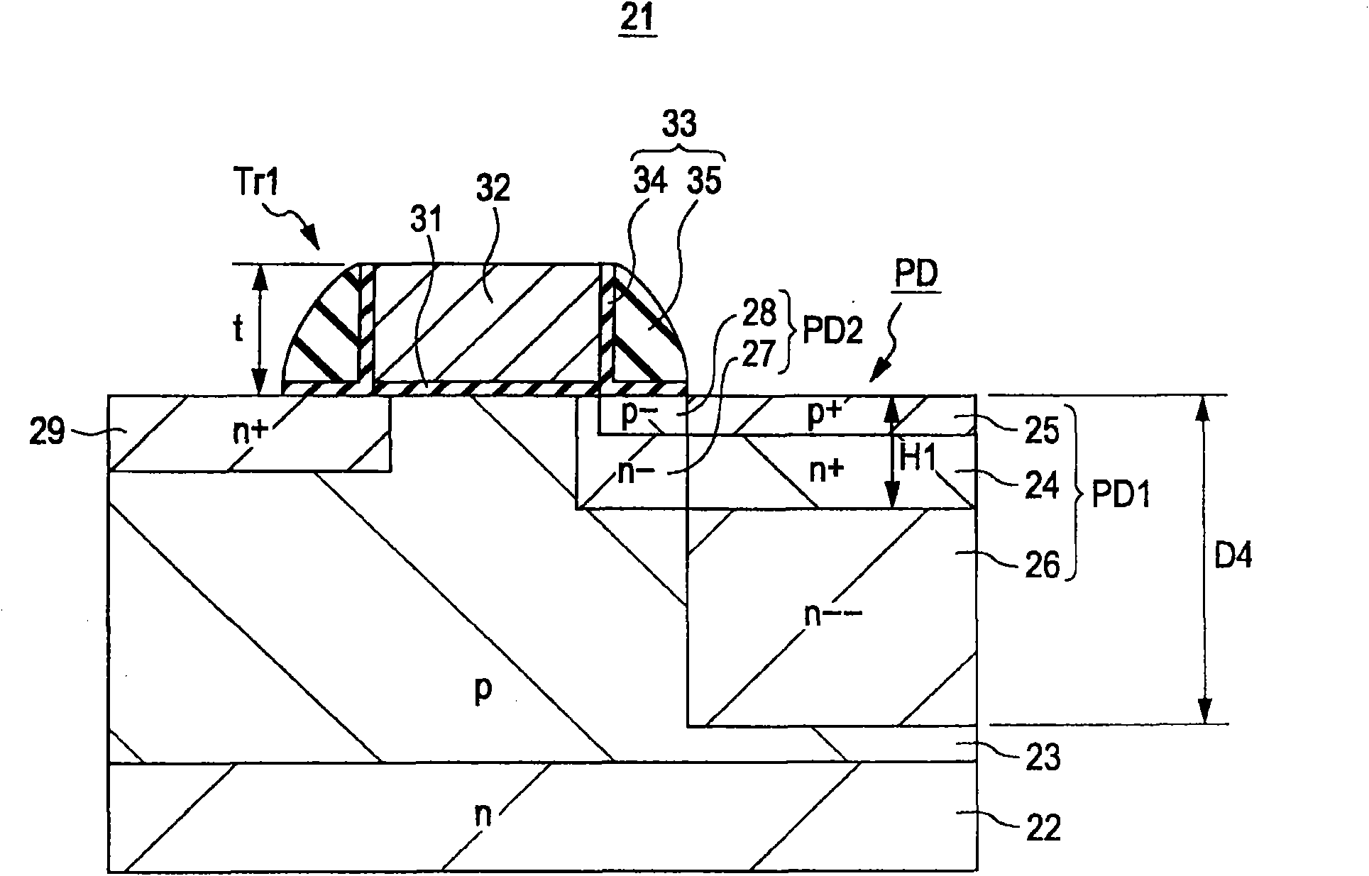
That is, when the hole charge storage region 107 approaches the transfer gate electrode 111, the gate voltage (read voltage) Vtg of the transfer transistor Tr1 increases, and thus it becomes difficult to read the signal charge
Method used
View moreImage
Smart ImageViewing Examples

Examples
no. 1 example
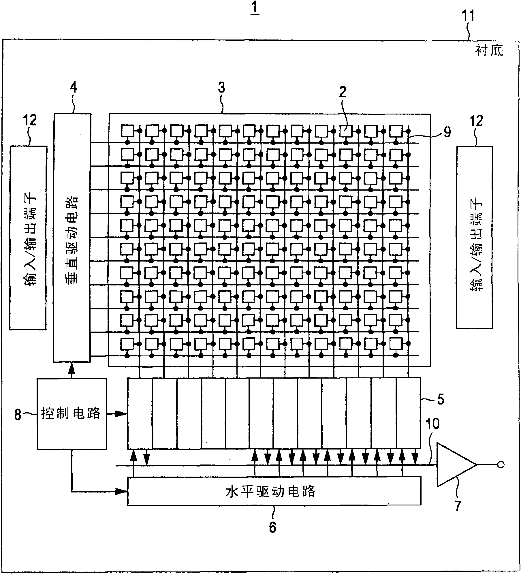
[0046] 2. First Embodiment (Exemplary Configuration of Solid-State Imaging Device and Exemplary Manufacturing Method Thereof)
no. 2 example
[0047] 3. Second Embodiment (Exemplary Configuration of Solid-State Imaging Device)
no. 3 example
[0048] 4. Third Embodiment (Exemplary Configuration of Solid-State Imaging Device)
Login to View More PUM
 Abstract
A solid-state imaging device includes plural photodiodes which are formed in a photodiode area of a unit pixel with no element separating area interposed therebetween and in which impurity concentrations of pn junction areas are different from each other.
Description
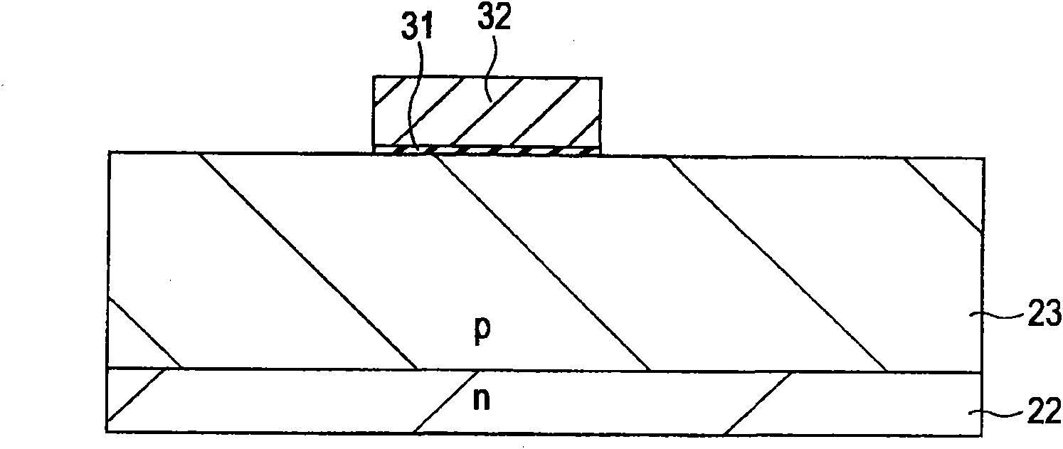
technical field [0001] The present invention relates to a solid-state imaging device, a method of manufacturing the same, and electronic equipment (such as a camera including the solid-state imaging device). Background technique [0002] As a solid-state imaging device, an amplifying type solid-state imaging device is known, a representative example of which is a MOS image sensor such as a CMOS (Complementary Metal Oxide Semiconductor) image sensor. In addition, there is also known a charge transport type solid-state imaging device, a representative example of which is a CCD (Charge Coupled Device) image sensor. These solid-state imaging devices are widely used in digital still cameras, digital video cameras, and the like. In recent years, for solid-state imaging devices mounted on cellular phones with cameras or PDAs (Personal Digital Assistants), MOS image sensors are widely used due to low voltage, low power consumption, and the like. [0003] In a MOS type solid-state ...
Claims
Login to View More Application Information
Patent Timeline
 Patent Type & AuthorityApplications(China)
IPC IPC(8): H01L27/146H01L31/08H01L31/0256H01L31/18H04N5/335H01L31/10
CPCH01L27/14627H01L27/14621H01L27/14643H01L27/14689H01L27/14609H01L31/103H01L27/14612H01L27/14605
Inventor糸长总一郎
OwnerSONY CORP