Display motherboard, manufacturing method thereof, and display device

A motherboard and column direction technology, applied in nonlinear optics, instruments, optics, etc., can solve the problems of different thicknesses, difficult diffusion and leveling of film layers, differences in pixel openings, etc., and achieve the effect of reducing film thickness differences.

Active Publication Date: 2018-09-04
BOE TECH GRP CO LTD +1
View PDF8 Cites 0 Cited by
  • Summary
  • Abstract
  • Description
  • Claims
  • Application Information

AI Technical Summary

Problems solved by technology

[0003] Currently, if figure 1 As shown, the motherboard 1 of MMG products often adopts the production method of large-size product 2 and small-size product 3. Due to the difference in product size, the pixel openings also have significant differences. In the panel manufacturing process, products of different sizes are due to equipment Limitation or consideration of the impact of production capacity requires a one-step process, which has caused some disadvantages. For example, in the process of manufacturing the color filter layer in the liquid crystal display panel, the R (red filter layer) process is usually carried out first, and then sequentially Carry out the G (green filter layer) process and B (blue filter layer) process, however, after the R (red filter layer) process, because its film thickness is greater than the thickness of the black matrix layer, under the influence of surface tension, In the subsequent process of other filter layers (such as G process or B process), the film layer formed by coating is not easy to diffuse and level, and because the degree of leveling has a large correlation with the size of the pixel opening of the product, the more pixel opening Smaller, the greater the film thickness formed in the pixel opening, resulting in different thicknesses of the same color filter layer in different sizes of products, for example, as figure 2 As shown, in the B (blue filter layer) process, since the size L1' of the pixel opening of the large-sized product 2 is larger than the size L2' of the pixel opening of the small-sized product 3, when the two are formed in the same step of the process, The film layer formed by coating is less likely to be diffused and leveled in small-sized products, so that the thickness d2' of the blue filter layer formed in small-sized products is greater than the thickness d1 of the blue filter layer formed in large-sized products '

Method used


Image

  • Display motherboard, manufacturing method thereof, and display device
  • Display motherboard, manufacturing method thereof, and display device
  • Display motherboard, manufacturing method thereof, and display device

Examples


Embodiment Construction

[0039] The specific implementation manners of the present invention will be further described in detail below in conjunction with the accompanying drawings and embodiments. The following examples are used to illustrate the present invention, but are not intended to limit the scope of the present invention.

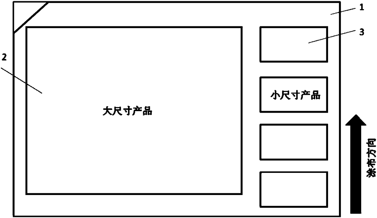
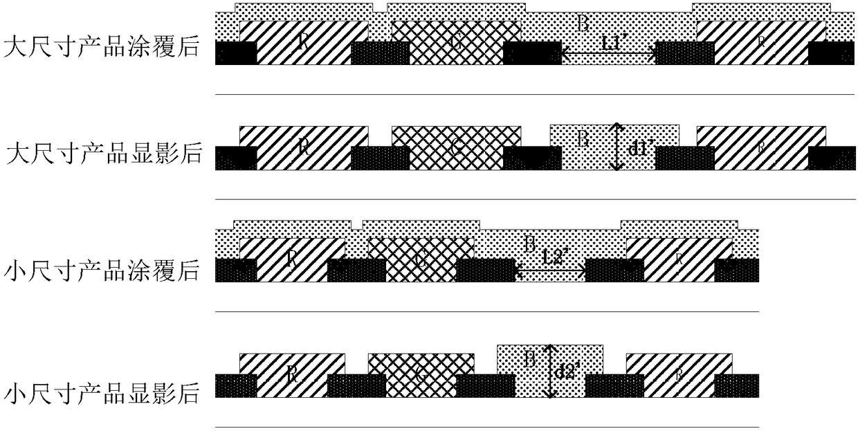
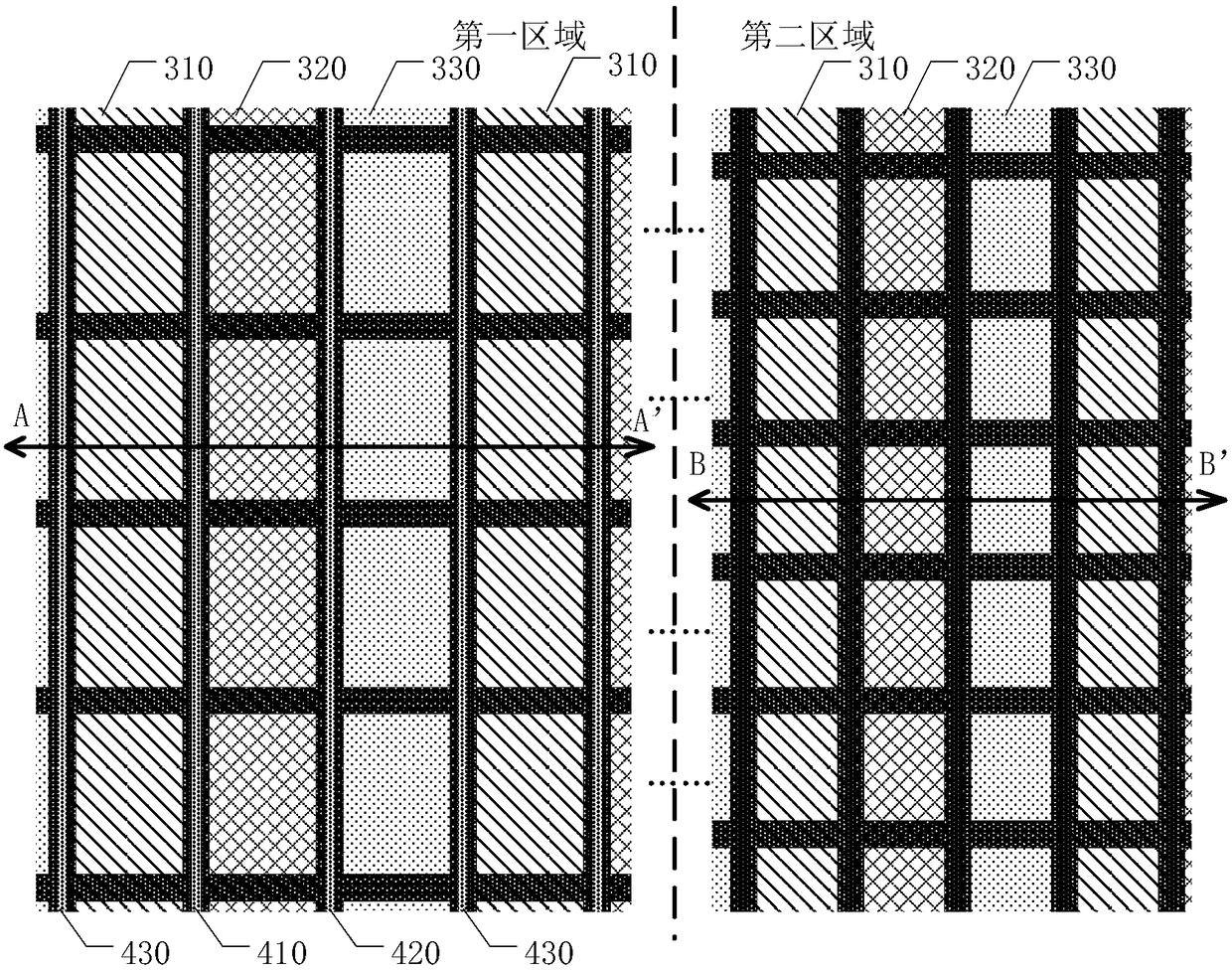
[0040] An embodiment of the present invention provides a display motherboard, which includes a base substrate, a black matrix layer and a color filter layer disposed on the base substrate, and the base substrate includes a first region and a second region. In the second area, the size of the sub-pixel opening area formed by the black matrix layer in the first area is larger than the size of the sub-pixel opening area formed by the black matrix layer in the second area, wherein the first area A retaining wall layer on the black matrix layer is also arranged on the top.

[0041] In the display motherboard provided by the embodiment of the present invention, by setting a bar...


PUM


Abstract

The invention provides a display motherboard, a production method thereof and a display device. The display motherboard comprises a substrate as well as a black matrix layer and a color filter layer which are arranged on the substrate, wherein the substrate comprises a first area and a second area; the size of each sub-pixel aperture area, formed in the first area, of the black matrix layer is larger than that of each sub-pixel aperture area, formed in the second area, of the black matrix layer; a retaining wall layer located on the black matrix layer is further arranged in the first area. According to the display motherboard, the retaining wall layer is arranged in the first area with larger sub-pixel apertures, so that the flowing resistance during photoresist coating can be increased through the retaining wall layer when the color filter layer is produced, and a film thickness difference of color filter layers in the same color due to a difference of pixel apertures of different sized products of MMG (multi-model glass) products can be reduced.

Description

technical field [0001] The invention relates to the display field, in particular to a display motherboard, a manufacturing method thereof, and a display device. Background technique [0002] With the development of liquid crystal display technology, people's demand for display products is getting higher and higher, and the requirements for types and models are also diverse. Among them, MMG (Multi-Model Glass, multi-model glass) technology is due to the combination of panels of different sizes Sleeve cutting on the same mother glass greatly improves the utilization rate of glass, so it is more and more used. [0003] Currently, if figure 1 As shown, the motherboard 1 of MMG products often adopts the production method of large-size product 2 and small-size product 3. Due to the difference in product size, the pixel openings also have significant differences. In the panel manufacturing process, products of different sizes are due to equipment Limitation or consideration of th...

Claims


Application Information

Patent Timeline
Patent Type & Authority Patents(China)
IPC IPC(8): G02F1/1335
CPCG02F1/133512G02F1/133514G02F1/133516
Inventor 杨同华冯贺万冀豫张思凯汪栋
Owner BOE TECH GRP CO LTD
Why Eureka
Try Eureka