
Image remapping method and device based on programmable logic device

A programming logic and remapping technology, which is applied in image data processing, graphics and image conversion, instruments, etc., can solve the problem of low bandwidth utilization of time-efficient memory, achieve the effect of saving internal storage and logic resources, and facilitating subsequent function integration

Active Publication Date: 2016-04-27
WUHAN JINGCE ELECTRONICS GRP CO LTD
View PDF4 Cites 10 Cited by
  • Summary
  • Abstract
  • Description
  • Claims
  • Application Information

AI Technical Summary

Problems solved by technology

[0003] At present, the remapping algorithm is generally implemented on the CPU or GPU (graphics processing unit). The algorithm needs to perform a large number of random reads on the image data in the DDR (external memory), and process the entire image at one time. Time efficiency and memory bandwidth very low utilization

Method used


Image

  • Image remapping method and device based on programmable logic device
  • Image remapping method and device based on programmable logic device
  • Image remapping method and device based on programmable logic device

Examples


Embodiment Construction

[0046] Below in conjunction with accompanying drawing and specific embodiment the present invention is described in further detail:

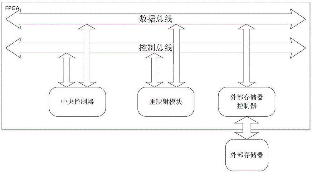
[0047] like figure 1 As shown, the structure of the image remapping device based on the programmable logic device of the present invention includes integrated in the programmable logic device:

[0048] Central controller: used to issue image parameters and remapping parameters to the remapping module;

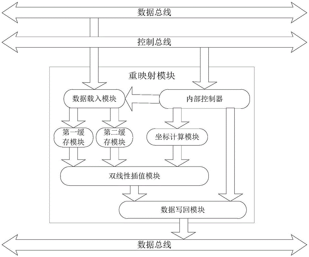
[0049]Remapping module: used to receive the image parameters and remapping parameters issued by the central controller, and calculate the block information of the image and the loading line address and write back line address of the image block, according to the loading line address of the image block from Load the image block into the external memory for remapping, and write the remapped image block data back to the external memory according to the write-back row address;

[0050] External memory controller: used to control the remapping modul...


PUM


Abstract

The invention relates to the technical field of TFT-LCD panel automatic optical inspection and specially relates to an image remapping method and device based on a programmable logic device. The method is characterized by dividing a target image into a plurality of image blocks; calculating an input line address and writing-back line address of each image block; carrying out remapping every time one image block is input according to the input line address of each image block, and writing back image data of the image blocks obtained after finishing remapping according to the corresponding writing-back line addresses; and inputting the next image block according to the input line address of the next image block and carrying out remapping until all of the image blocks of the target image finish remapping. The method is realized based on the FPGA, and is characterized by dividing the target image into the plurality of image blocks and inputting the image blocks one by one for processing, thereby saving storage and logic resources in the FPGA and facilitating integration of follow-up functions.

Description

technical field [0001] The invention relates to the technical field of automatic optical detection of TFT-LCD panels, in particular to an image remapping method and device based on a programmable logic device. Background technique [0002] Image remapping algorithm (Remap) is an important image processing algorithm, which is widely used in image transformation processing. The remapping algorithm has become the core algorithm for image scaling, rotation, translation, distortion and other operations. In the process of automatic optical inspection of TFT-LCD (ThinfilmtransistorLiquidcrystaldisplayLCD, Thinfilm Transistor Liquid Crystal Display) panels, it is first necessary to perform distortion correction and geometric correction on the target image captured by the industrial camera. The core operation of distortion correction and geometric correction is to reconstruct the image. map. [0003] At present, the remapping algorithm is generally implemented on the CPU or GPU (gr...

Claims


Application Information

Patent Timeline
Patent Type & Authority Applications(China)
IPC IPC(8): G06T3/00
CPCG06T3/00
Inventor 梅林海欧昌东汪舟简平超董文忠
Owner WUHAN JINGCE ELECTRONICS GRP CO LTD
Learn More