Array substrate, display panel, methods for preparing array substrate and display panel, and display device

A technology for array substrates and display panels, which is applied in the direction of instruments, semiconductor devices, optics, etc., can solve the problems of poor sealability of the sealing glue and the bonded film layer, so as to avoid the influence of adhesion force and keep the seal performance, the effect of good sealing performance

Active Publication Date: 2016-05-04
BOE TECH GRP CO LTD +1
View PDF6 Cites 3 Cited by
  • Summary
  • Abstract
  • Description
  • Claims
  • Application Information

AI Technical Summary

Problems solved by technology

[0005] The purpose of the present invention is to provide an array substrate, a display panel and its corresponding preparation method and a display device, so as to solve the problem of the organic film layer under the frame sealant being affected by the environment of high temperature, high pressure and high humidity, resulting in the failure of the frame sealant. The problem of poor sealing between the bonded film layers

Method used


Image

  • Array substrate, display panel, methods for preparing array substrate and display panel, and display device
  • Array substrate, display panel, methods for preparing array substrate and display panel, and display device
  • Array substrate, display panel, methods for preparing array substrate and display panel, and display device

Examples


preparation example Construction

[0054] see Figure 4 , an embodiment of the present invention provides a method for preparing an array substrate, including:

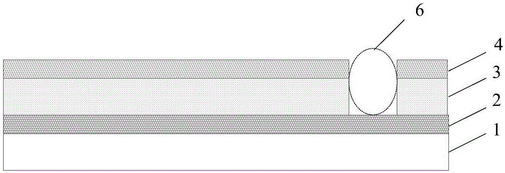
[0055] 401. Form a gate protection layer, an organic film layer, and an insulating layer in sequence on a base substrate.

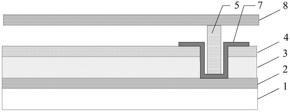
[0056] 402. Form a groove structure through a patterning process at a position for setting the sealant; wherein, the groove structure extends from the insulating layer to the gate protection layer in a direction perpendicular to the substrate, and exposes the gate protection layer.

[0057] preferred, see Figure 5 , the embodiment of the present invention provides another method for preparing an array substrate, including:

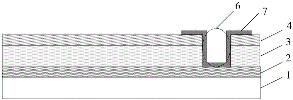
[0058] 501. Form a gate protection layer, an organic film layer, and an insulating layer in sequence on a base substrate.

[0059] 502. At the position for setting the sealant, form a groove structure through a patterning process; wherein, the groove structure extends from the insulating layer to the gate ...


PUM


Abstract

The invention aims to provide an array substrate, a display panel, methods for preparing the array substrate and the display panel, and a display device to solve the problem that when an organic membrane under a seal agent is affected by high temperature, high pressure and high humidity, sealing property between the seal agent the membrane adhering to the seal agent becomes poor. The array substrate comprises a substrate body, a grid protection layer, an organic membrane and an insulating layer, wherein the grid protection layer, the organic membrane and the insulating layer are sequentially formed on the substrate body. A groove structure used for accommodating a seal agent is formed in the array substrate and extends towards the grid protection layer from the insulating layer in the direction perpendicular to the substrate, and the grid protection layer is exposed.

Description

technical field [0001] The invention relates to the field of liquid crystal display, in particular to an array substrate, a display panel, a corresponding preparation method thereof, and a display device. Background technique [0002] Thin Film Transistor Liquid Crystal Display (TFT-LCD) has the characteristics of small size, low power consumption, no radiation, and relatively low manufacturing cost, and occupies a dominant position in the current flat panel display market. [0003] TFT-LCD includes array substrate, color filter substrate and liquid crystal between them. Wherein, the liquid crystal between the array substrate and the color filter substrate is sealed by a sealant. The array substrate generally includes an insulating layer, an organic film layer, a gate protection layer, a gate metal layer, etc. below the position where the sealant is disposed. [0004] However, when in the environmental conditions of high temperature, high pressure and high humidity, the la...

Claims


Application Information

Patent Timeline
IPC IPC(8): G02F1/1333G02F1/1339G02F1/1343
CPCG02F1/1333G02F1/1339G02F1/1343G02F1/13439G02F1/1362G02F1/0107G02F1/13625G02F1/133345G02F1/133514H01L27/127
Inventor 周纪登张伟
Owner BOE TECH GRP CO LTD
Why Eureka
Try Eureka