Chip programming system, method, and electronic device

A burning method and technology of electronic equipment system, applied in the field of chip program burning, can solve problems such as test and development personnel's time occupation, speed and development mode bottleneck, and slow command execution speed, so as to reduce the probability of bad burning and save Development time, effect of reducing development time

Active Publication Date: 2020-01-17
HEFEI CHIPSEA ELECTRONICS TECH CO LTD
View PDF9 Cites 1 Cited by
  • Summary
  • Abstract
  • Description
  • Claims
  • Application Information

AI Technical Summary

Problems solved by technology

[0002] The current chip programming platform is developed based on the Silicon Laboratories IDE of C51. Its single download code interface, slow download speed and no information prompts bring difficulties to users, low operating frequency, slow command execution speed and poor portability. It is not conducive to the maintenance and program upgrade of subsequent developers; the time for burning chips is too long, which affects production capacity, and the error rate of burning chips is high (greater than 5 per thousand), which affects customer experience; it is necessary to purchase a dedicated USB chip separately , the speed of transmission is limited in a large program, resulting in the bottleneck of speed and development mode, and the development of PC software is limited by the API functions provided by USB FIFO manufacturers, which has poor operability and versatility, resulting in high development and maintenance costs; burning The automation level of the recording device platform is low, and the burning cannot automatically detect whether the chip is online, whether the chip pins are aligned, and there is no overvoltage and overcurrent on the hardware circuit, which will lead to bad programming of the chip, and manual operation of the software is required. As a result, a large amount of time is taken up by test developers, and it is difficult to have enough energy and time to do other work and improve technical capabilities

Method used


Image

  • Chip programming system, method, and electronic device
  • Chip programming system, method, and electronic device
  • Chip programming system, method, and electronic device

Examples


Embodiment Construction

[0038] In order to make the object, technical solution and advantages of the present invention more clear, the present invention will be further described in detail below in conjunction with the accompanying drawings and embodiments. It should be understood that the specific embodiments described here are only used to explain the present invention, not to limit the present invention.

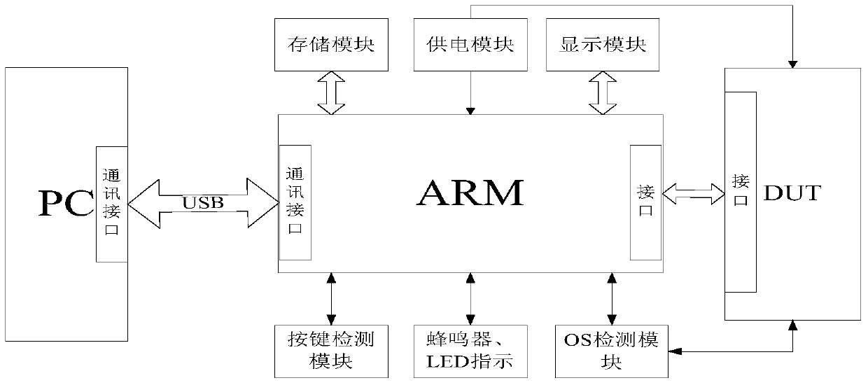
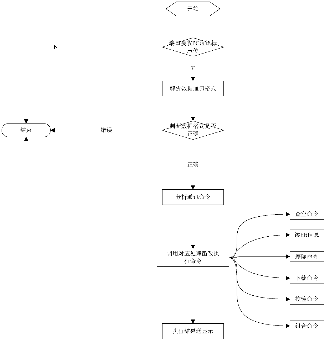
[0039] Please refer to figure 1 As shown, in order to solve the above technical problems, the present invention firstly provides an electronic equipment system for chip programming, which can perform automatic programming for internal personnel and customers, and improve the efficiency of programming. The electronic equipment system developed by the present invention supports two modes of online burning and offline burning. Online burning means that the user connects the terminal of the electronic equipment system to the PC end, and completes the burning operation through the PC coordination con...


PUM


Abstract

The invention discloses an electronic equipment system for burning a chip and a burning method. The system comprises a USB communication module, a detection output module, a UI display alarm module, a firmware upgrade module, a storage module, a PC control software module and a key module, wherein the modules are in connection or communication with an ARM respectively; and burning of the chip is achieved through the system. The system and the method disclosed by the invention can achieve quick burning of the chip at relatively low cost, can carry out burning in different modes, and prompts a user to automatically detect chip placement by different information in the burning process. By a software-hardware coordinated development mode, the development time can be greatly shortened; and the probability of poor burning caused by a contact problem is lowered.

Description

technical field [0001] The invention relates to chip program burning of an ARM-based 32-bit MCU, in particular to a chip burning method for automatically detecting whether a chip is online during design. Background technique [0002] The current chip programming platform is developed based on the Silicon Laboratories IDE of C51. Its single download code interface, slow download speed and no information prompts bring difficulties to users, low operating frequency, slow command execution speed and poor portability. It is not conducive to the maintenance and program upgrade of subsequent developers; the time for burning chips is too long, which affects production capacity, and the error rate of burning chips is high (greater than 5 per thousand), which affects customer experience; it is necessary to purchase a dedicated USB chip separately , the speed of transmission is limited in a large program, resulting in the bottleneck of speed and development mode, and the development of...

Claims


Application Information

Patent Timeline
Patent Type & Authority Patents(China)
IPC IPC(8): G06F9/4401
CPCG06F9/4411
Inventor 庞新洁
Owner HEFEI CHIPSEA ELECTRONICS TECH CO LTD
Why Eureka
Try Eureka