Tray wafer positioning system, method and mocvd equipment

A positioning method and positioning system technology, applied in the semiconductor field, can solve problems such as unstable rotation of the tray, uneven weight distribution of the wafer, and reduced uniformity of film growth

Active Publication Date: 2017-12-29
TANG OPTOELECTRONICS EQUIPMENT (SHANGHAI) CORPORATION LIMITED
View PDF5 Cites 0 Cited by
  • Summary
  • Abstract
  • Description
  • Claims
  • Application Information

AI Technical Summary

Problems solved by technology

[0004] The first one is to position the wafer through the position of the motor encoder; the disadvantage is that there must be a rigid connection between the tray and the rotating shaft that supports and drives it to rotate, and this method cannot be used for non-rigidly connected trays.
[0008] The disadvantage is that in this method, the wafers in a certain area on the tray are asymmetrically discharged, which may lead to uneven weight distribution of the wafers on the tray, and cause unstable tray rotation when the tray rotates at a high speed, which is more likely to cause Reduced film growth uniformity between wafers throughout the run

Method used


Image

  • Tray wafer positioning system, method and mocvd equipment
  • Tray wafer positioning system, method and mocvd equipment
  • Tray wafer positioning system, method and mocvd equipment

Examples


Embodiment Construction

[0068] A method for positioning a wafer on a tray provided in an embodiment of the present invention, which includes the following steps:

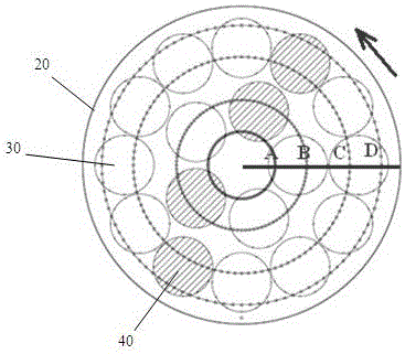
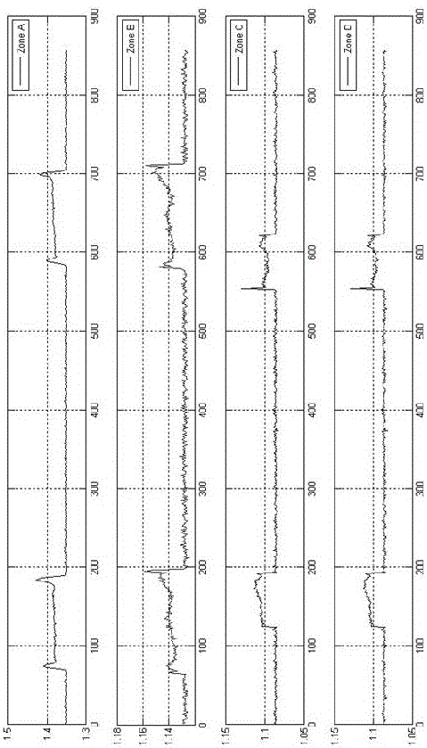
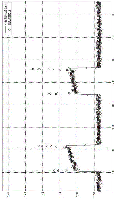
[0069] When the tray rotates, measure optical signals corresponding to at least two circles of wafers on the tray to obtain at least two sets of optical signal sequences;

[0070] Matching the measured at least two groups of optical signal sequences as a whole with the preset position information template; the position information template includes the corresponding position information templates of the at least two circles of wafers, and each circle of wafers The corresponding position information template includes the number of each groove in the corresponding circle of grooves, the coordinate information of each groove, and the wafer placement information in each groove;

[0071] Find out the positions of the optical signals corresponding to each circle of wafers in their respective sequences when the matching degree is the highest, and...


PUM


Abstract

The invention relates to a tray wafer positioning system, method and MOCVD system. When the tray rotates, the optical signals corresponding to at least two circles of wafers on the tray are measured to obtain at least two sets of optical signal sequences; the measured at least two sets of As a whole, the optical signal sequence is matched with the position information template including the tray position information and wafer placement information; find out the position of the optical signal corresponding to each circle of wafers in the respective sequence when the matching degree is the highest, and then determine the position on the tray. The number of each wafer in each circle of wafers. In the case that the hardware setting itself cannot provide an effective positioning signal, the present invention relies on the characteristics of the position of the groove on the tray to process and analyze the collected optical signal to realize the absolute positioning of each wafer on the tray, and then the collected The data of each wafer is divided to obtain the data corresponding to each wafer.

Description

technical field [0001] The invention relates to the field of semiconductors, in particular to a tray wafer positioning system, method and MOCVD equipment. Background technique [0002] Chemical vapor deposition equipment, such as metal organic chemical vapor deposition (MOCVD) equipment is one of the core equipment for the production of semiconductor optoelectronic devices, and is used to deposit or epitaxially grow crystal structure films on wafers (or epitaxial wafers or substrates). The reaction chamber of the MOCVD equipment is provided with a tray, the tray is generally made of graphite, and there are multiple circles of grooves arranged on it for correspondingly placing the wafer. [0003] At present, there are the following methods for positioning wafers on the tray: [0004] The first is to position the wafer through the position of the motor encoder; the disadvantage is that there must be a rigid connection between the tray and the rotating shaft that supports and ...

Claims


Application Information

Patent Timeline
Patent Type & Authority Patents(China)
IPC IPC(8): C23C16/18C23C16/458C30B25/12
Inventor 黄玉峰马法君徐春阳赵辉
Owner TANG OPTOELECTRONICS EQUIPMENT (SHANGHAI) CORPORATION LIMITED
Why Eureka
Try Eureka