Atomic force microscope and surface photovoltage spectrum combination method

A technology of surface photovoltage spectroscopy and atomic force microscopy, which is applied to the measurement of electrical variables, measuring devices, instruments, etc., can solve the problems of lack of spatial resolution of surface photovoltage spectroscopy, limitations of surface photovoltage spectroscopy, and unavailability

Active Publication Date: 2016-06-01
DALIAN INST OF CHEM PHYSICS CHINESE ACAD OF SCI
View PDF4 Cites 4 Cited by
  • Summary
  • Abstract
  • Description
  • Claims
  • Application Information

AI Technical Summary

Problems solved by technology

However, the surface photovoltage spectrum lacks spatial resolution, especially when studying the above problems, it involves the distribution of charges in the range of nanometers and micrometers, and the application of surface photovoltage spectroscopy is greatly limited.
The atomic force microscope can obtain nanometer-resolution spatial information, and can also obtain nanometer-resolution electrical signals, such as surface potential, capacitance, etc., but the atomic force microscope itself cannot obtain the information of these signals changing with the excitation wavelength

Method used


Image

  • Atomic force microscope and surface photovoltage spectrum combination method
  • Atomic force microscope and surface photovoltage spectrum combination method
  • Atomic force microscope and surface photovoltage spectrum combination method

Examples


Embodiment approach

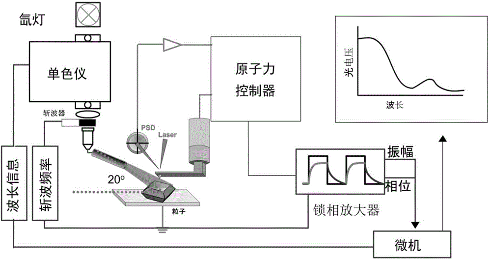
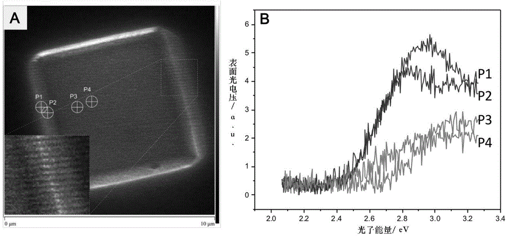
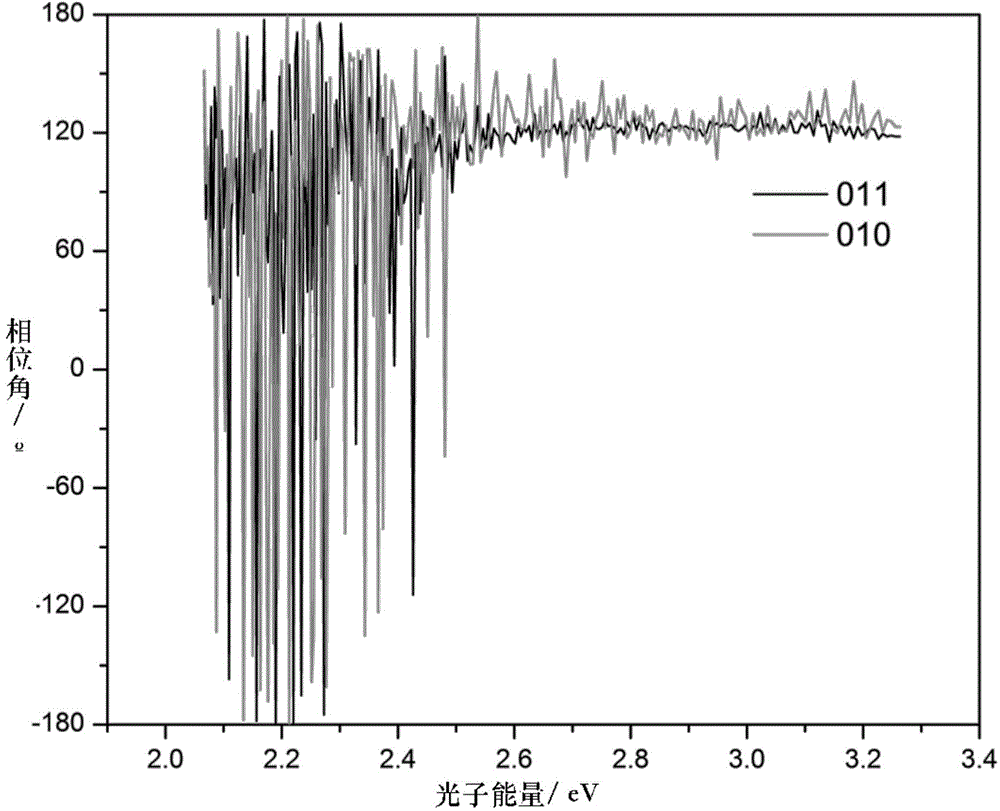
[0018] 1 BiVO 4 The particles were fixed on the FTO conductive glass by spin coating, and washed with ethanol and secondary water in sequence. Dry on a hot table at 70°C;

[0019] 2. Turn on the atomic force microscope and scan the shape first to find the particles to be tested. Select the area to be tested and continuously narrow the scanning range until the scanning range approaches 0 nanometers;

[0020] 3 Open the atomic force surface potential output interface, and set the output signal on the front panel of the atomic force controller to electric potential. Input this signal to the signal input terminal of the lock-in amplifier;

[0021] 4 Turn on the monochromator, turn on the xenon lamp, and select 380 nm as the initial scanning wavelength.

[0022] 5 Turn on the chopper, set the frequency to 6 Hz, and input the chopper frequency signal to the lock-in amplifier;

[0023] 6 Connect the amplitude and phase signals obtained by the lock-in amplifier to the data acquis...


PUM


Abstract

The invention relates to an atomic force microscope and surface photovoltage spectrum combination method for measuring a surface photovoltage spectrum of a semiconductor surface micro region to solve the problem that the surface photovoltage spectrum has no spatial resolving power. An atomic force microscope and a spectrometer are combined by using a chopper for modulating a variable wavelength signal and combining the surface potential variation with a lock-in amplifier, and the surface photovoltage spectrum of the semiconductor surface micro region and a phase angle resolution spectrogram can be given.

Description

technical field [0001] The invention relates to a combined method of atomic force microscope and surface photovoltage spectrum, which is applicable to the surface photovoltage spectrum measurement of micron and nanometer regions on the surface of semiconductor particles. Background technique [0002] Photocatalytic water splitting to produce hydrogen is an important way to develop and utilize solar energy. For solar hydrogen and CO 2 Due to the great demand for reduction, people are developing a series of synthesis methods and assembly strategies for photocatalytic materials, including the modification of nanostructures on the surface of semiconductor catalysts, the directional synthesis of crystal planes, the synthesis of low-dimensional structures, and the construction of heterojunctions / heterojunctions The assembly strategy of co-catalyst and co-catalyst improves the efficiency of photoelectrocatalytic water splitting to a certain extent. However, so far, people's under...

Claims


Application Information

Patent Timeline
Patent Type & Authority Applications(China)
IPC IPC(8): G01R29/00
Inventor 李灿朱剑范峰滔安虹宇陈若天
Owner DALIAN INST OF CHEM PHYSICS CHINESE ACAD OF SCI
Why Eureka
Try Eureka