PMOS transistor forming method

A transistor and gas technology, applied in the field of formation of PMOS transistors, can solve the problems of unstable performance of PMOS transistors, saturation leakage current drift, large leakage current, etc., and achieve the effect of solving the problem of unstable performance.

Active Publication Date: 2016-06-01
SEMICON MFG INT (SHANGHAI) CORP
View PDF4 Cites 1 Cited by
  • Summary
  • Abstract
  • Description
  • Claims
  • Application Information

AI Technical Summary

Problems solved by technology

[0003] In the actual process, it is found that the PMOS transistors manufactured above often have large leakage currents, and the performance of multiple PMOS transistors manufactured in the same batch is unstable, such as saturation leakage current drift and other problems.

Method used


Image

  • PMOS transistor forming method
  • PMOS transistor forming method
  • PMOS transistor forming method

Examples


Embodiment Construction

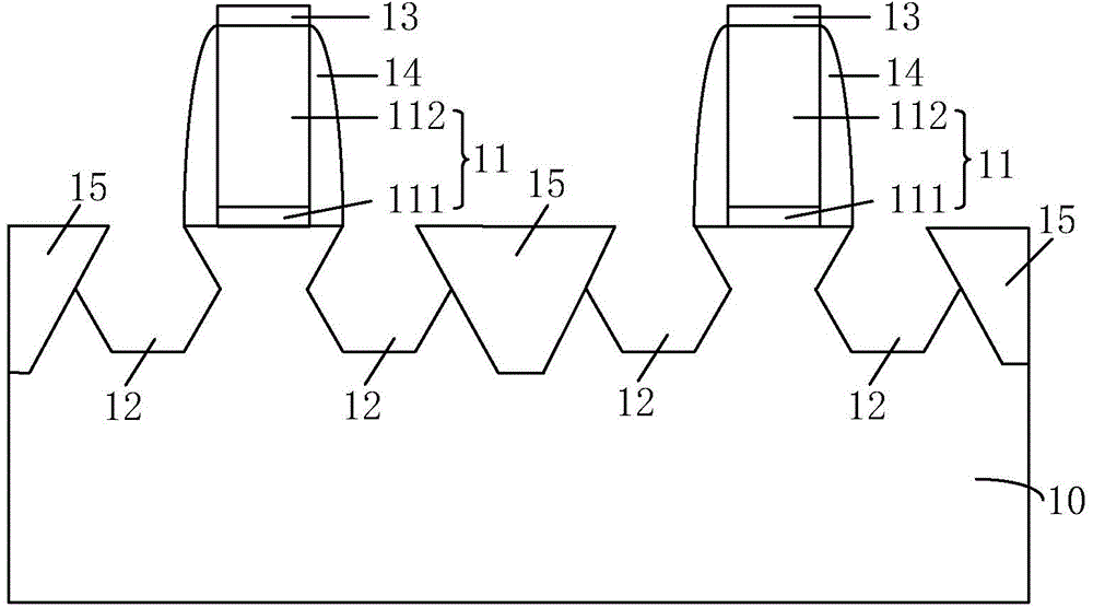
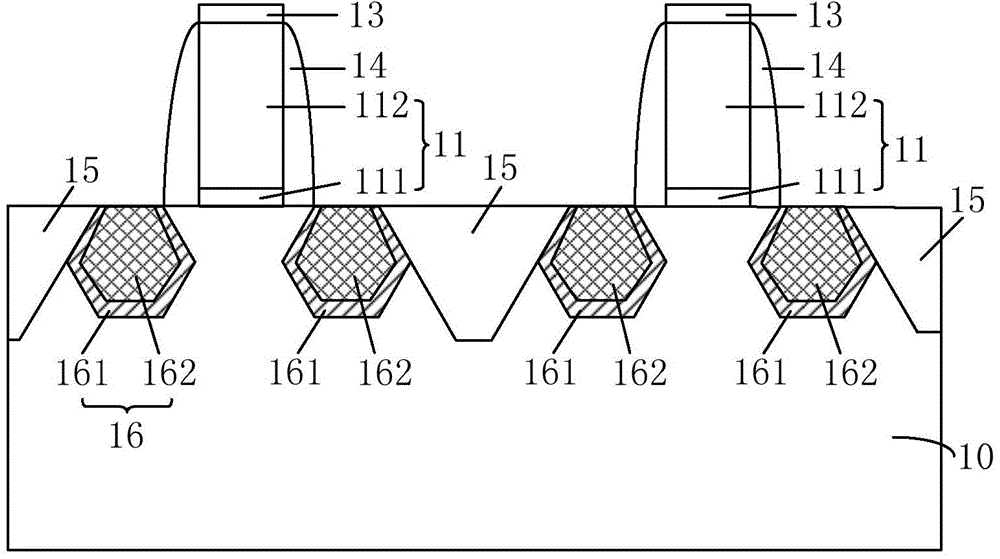
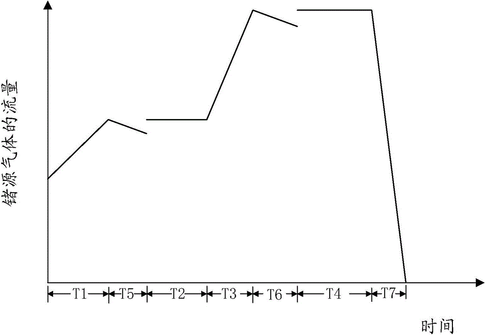
[0030] As described in the background art, the leakage current of PMOS transistors manufactured by the prior art is relatively large, and the performance of multiple PMOS transistors manufactured in the same batch is unstable. In view of the above problems, the inventors have analyzed and found that the reason is: for the formation stage of the silicon germanium seed layer in the sigma-shaped groove, the first sub-stage when the germanium source gas flow rate gradually increases and the gas flow rate is stable At the junction of the second sub-stage, the sudden change in the flow rate of the germanium source gas will cause the germanium content in the formed silicon germanium seed layer to suddenly increase, causing the silicon germanium material in the silicon germanium seed layer to be mismatched in the lattice, and then causing the sigma shape Defects appear on the sidewalls of the groove, and carriers in the source and drain regions enter the channel region to cause leakage ...


PUM


Abstract

The invention discloses a PMOS transistor forming method. The method comprises the steps: adding a fifth subphase that the flow gradually decreases between a first subphase that a germanium source gas flow gradually increases and a second subphase that the flow is table for a phase that silicon germanium seed crystal is formed in a sigma groove of a source-drain region, wherein the initial flow of germanium source gas at the fifth subphase is equal to the tail flow of the first subphase; and/or adding a sixth subphase that the flow gradually decreases between a third subphase that a gas flow gradually increases and a fourth subphase that the flow is table for a phase that a bulk material is formed, wherein the initial flow of germanium source gas at the sixth subphase is equal to the tail flow of the third subphase. The method can the flow abrupt changes at the joint of the first and second subphases and/or the joint of the third and fourth subphases from causing the abrupt increase of the content of germanium in a formed silicon germanium material, avoids the mismatching of the silicon germanium material crystal lattices, and avoids current leakage caused by that carriers of the source-drain regions enter a trench region because of the recessing of a side wall of the sigma groove.

Description

Technical field [0001] The present invention relates to the technical field of semiconductor manufacturing, in particular to a method for forming a PMOS transistor. Background technique [0002] In the existing semiconductor device manufacturing process, since stress can change the energy gap and carrier mobility of silicon materials, improving the performance of MOS transistors through stress has become an increasingly common method. Specifically, a sigma-shaped groove is formed in the source / drain region of the transistor, and compressive stress or tensile stress material is filled in it, and the tip of the sigma-shaped groove is used to apply compressive or tensile stress to the channel, thereby improving the groove The mobility of carriers in the channel (electrons in NMOS transistors, holes in PMOS transistors). [0003] In the actual process, it is found that the PMOS transistors manufactured above often have large leakage currents, and the performance of multiple PMOS trans...

Claims


Application Information

Patent Timeline
Patent Type & Authority Applications(China)
IPC IPC(8): H01L21/336
Inventor 涂火金
Owner SEMICON MFG INT (SHANGHAI) CORP
Why Eureka
Try Eureka