Electrochemical treatment method for improving surface properties of copper indium gallium selenide thin film
A technology of copper indium gallium selenide and surface properties, which is applied in the field of solar cells, can solve the problems of easy introduction of other impurities, serious environmental pollution, complicated operation, etc., and achieves the effects of environmental friendliness, stable solution system, and high recycling rate.
- Summary
- Abstract
- Description
- Claims
- Application Information
AI Technical Summary
Problems solved by technology
Method used
Image

Examples
Embodiment 1
[0043] Example 1 This example is an electrochemical method to etch the surface of a copper indium gallium selenide film
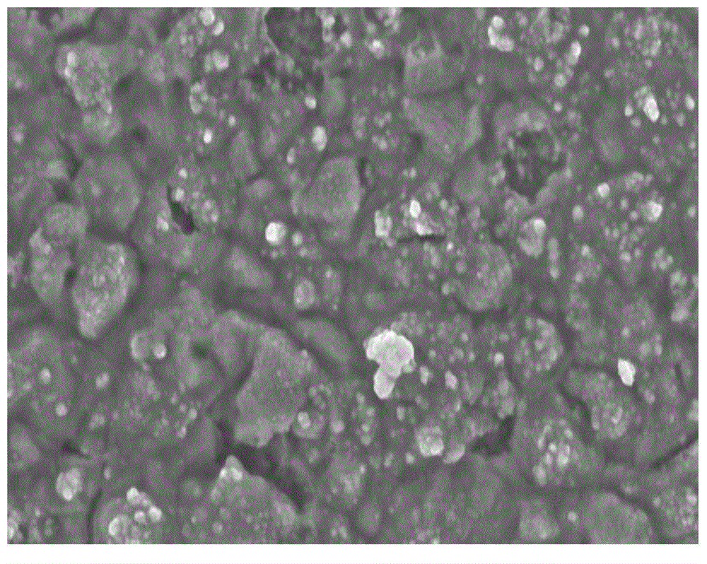
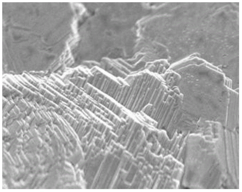
[0044] Metal Mo with a thickness of 1 μm is deposited on the soda-lime glass, and a copper indium gallium selenide film 2 with a thickness of 1 μm is deposited on the Mo layer 4 by electrochemical deposition, and then annealed in a quartz tube furnace. The scanning electron microscope image of the copper indium gallium selenide thin film 2 after selenization is shown in figure 2 .
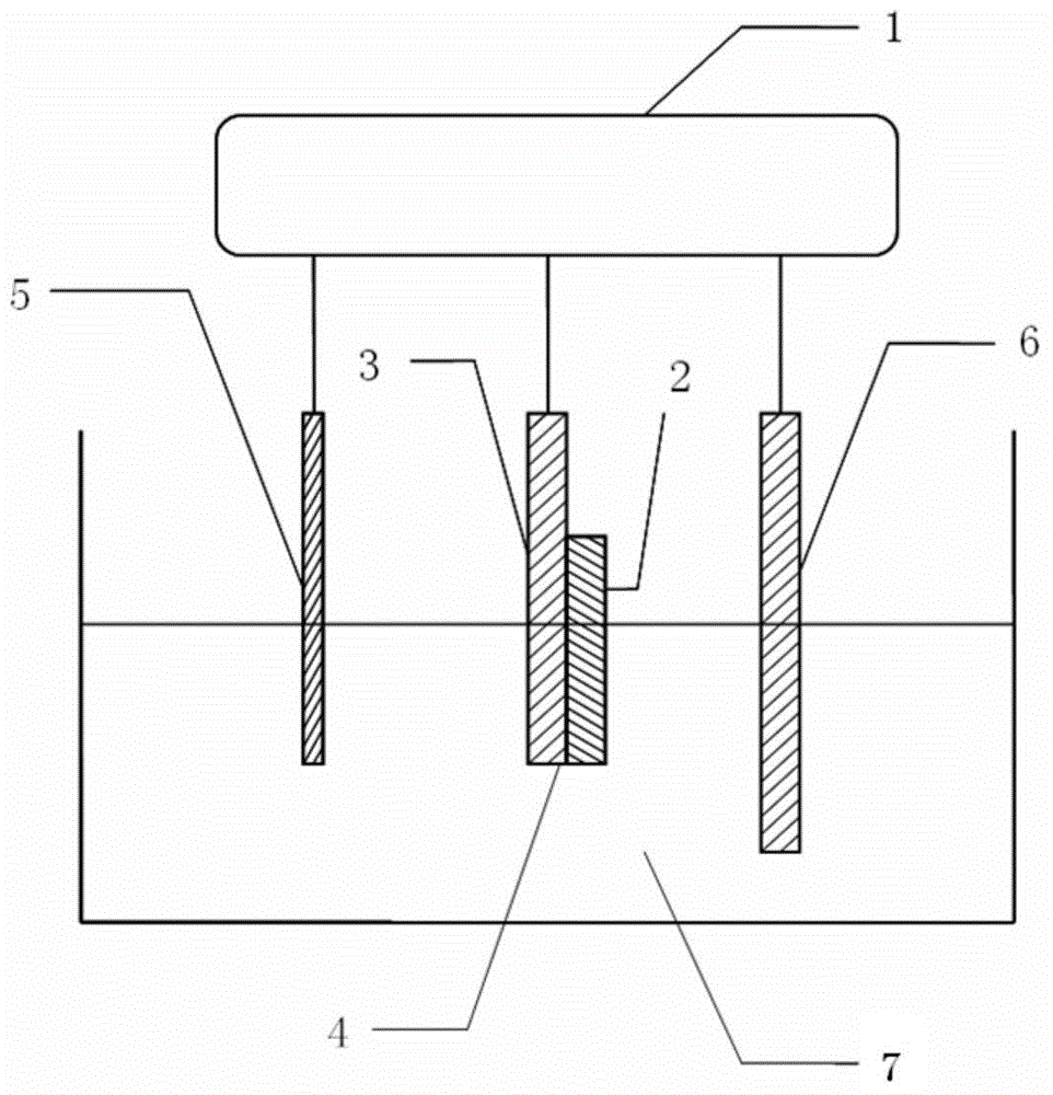
[0045] Step (1): Connect the selenized copper indium gallium selenide thin film 2 to the working electrode of the electrochemical workstation 1, the connecting part is only the Mo layer 4, soak in absolute ethanol solution for 1 to 2 minutes, remove the surface stained with particulate impurities;
[0046] Step (2): preparation treatment solution 7, treatment solution 7 is the mixed solution of potassium sulfite, potassium sulfide and deionized water, the concentration of pot...
Embodiment 2
[0049] Example 2 This example is an electrochemical method to etch the surface of the copper indium gallium selenide film
[0050] Metal Mo with a thickness of 1 μm is deposited on the soda lime glass, and a copper indium gallium selenide film 2 with a thickness of 1 μm is deposited on the Mo layer 4 by pulse electrochemical deposition, and then annealed in a quartz tube furnace.
[0051] Step (1): Connect the selenized copper indium gallium selenide thin film 2 to the working electrode of the electrochemical workstation 1, the connecting part is only the Mo layer 4, soak in absolute ethanol solution for 1 to 2 minutes, remove the surface stained with particulate impurities;
[0052] Step (2): Prepare treatment solution 7, treatment solution 7 is a mixed solution of sodium sulfite, sodium sulfide and deionized water, the concentration of sodium sulfite in the mixed solution is 0.25M / L, and the concentration of sodium sulfide in the mixed solution is 0.35M / L, pH=13;
[0053]...
Embodiment 3
[0055] Example 3 This example is an electrochemical method to etch the surface of the copper indium gallium selenide film
[0056] Metal Mo with a thickness of 1 μm is deposited on the soda lime glass, and a copper indium gallium selenide film 2 with a thickness of 1 μm is deposited on the Mo layer 4 by pulse electrochemical deposition, and then annealed in a quartz tube furnace.
[0057] Step (1): Connect the selenized copper indium gallium selenide thin film 2 to the working electrode of the electrochemical workstation 1, the connecting part is only the Mo layer 4, soak in absolute ethanol solution for 1 to 2 minutes, remove the surface stained with particulate impurities;
[0058] Step (2): preparation treatment solution 7, treatment solution 7 is the mixed solution of potassium sulfite, sodium sulfide and deionized water, the concentration of potassium sulfite in the mixed solution is 0.25M / L, the concentration of sodium sulfide in the mixed solution The concentration is ...
PUM
 Abstract
Description
Claims
Application Information
 - R&D Engineer
- R&D Manager
- IP Professional
- Industry Leading Data Capabilities
- Powerful AI technology
- Patent DNA Extraction
Browse by: Latest US Patents, China's latest patents, Technical Efficacy Thesaurus, Application Domain, Technology Topic.
© 2024 PatSnap. All rights reserved.Legal|Privacy policy|Modern Slavery Act Transparency Statement|Sitemap