TEM sample preparation method

A sample and sample stage technology, which is applied in the field of transmission electron microscope sample preparation, can solve the problems of reducing the success rate of sample preparation, prolonging the sample preparation cycle, and sample fragmentation, so as to improve the success rate of sample preparation, shorten the sample preparation cycle, The effect of reducing the preparation cycle

Active Publication Date: 2016-06-08
NORTHWESTERN POLYTECHNICAL UNIV
View PDF7 Cites 8 Cited by
  • Summary
  • Abstract
  • Description
  • Claims
  • Application Information

AI Technical Summary

Problems solved by technology

This method increases the sample success rate from 30%-40% of the background technology to 60%-70%, but the sample preparation period of this method is very long, at least 20h is required. In addition, because the sample is first bonded to the copper ring and then ground If it is less than 50μm, this process will easily lead to sample fragmentation and reduce the success rate of...

Method used


Image

  • TEM sample preparation method
  • TEM sample preparation method
  • TEM sample preparation method

Examples


Embodiment 1

[0025] This embodiment is a TEM sample preparation method, the specific process is:

[0026] The first step is to prepare the primary sample: use diamond wire cutting to cut the primary sample from the CdZnTe wafer, the size is 3×3×2mm 3 , a total of 4 pieces, use alcohol to clean the wafer, and obtain 4 samples to be used;

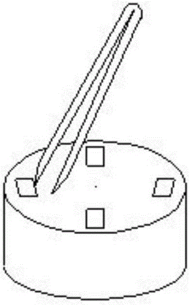
[0027] The second step, preliminary thinning of the primary sample: use MTICorporation's HEATINGPLATE-250 model heating platform, set the temperature at 90°C, place a cylindrical sample platform with a specification of Φ40mm×15mm on the heating platform, preheat for 4 to 8 minutes, and use The surface of the sample stage was coated with a paraffin stick, and 4 primary samples were placed on the surface of the sample stage coated with paraffin; the sample stage was removed from the heating stage, and naturally cooled at room temperature for 12-15 minutes. Use 2000# sandpaper to grind and thin the sample for 5-10 minutes, then use 5000# sandpaper to grind ...

Embodiment 2

[0034] This embodiment is a TEM sample preparation method, the specific process is:

[0035] The first step is to prepare the primary sample: use diamond wire cutting to cut the primary sample from the CdZnTe wafer, the size is 3×3×2mm 3 , a total of 8 pieces, use alcohol to clean the wafer, and obtain 8 samples to be used;

[0036] The second step, preliminary thinning of the primary sample: use MTICorporation's HEATINGPLATE-250 model heating platform, set the temperature at 90°C, place a cylindrical sample platform with a specification of Φ40mm×15mm on the heating platform, preheat for 4-8min, and use Smear the surface of the sample stage with a paraffin stick, and place 8 primary samples on the surface of the sample stage coated with paraffin; remove the sample stage from the heating stage, and let it cool naturally at room temperature for 12-15 minutes. Use 2000# sandpaper to grind and thin the sample for 5-10 minutes, then use 5000# sandpaper to grind and thin the sample...

Embodiment 3

[0043] This embodiment is a TEM sample preparation method, the specific process is:

[0044] The first step is to prepare the primary sample: use diamond wire cutting to cut the primary sample from the CdZnTe wafer, the size is 3×3×2mm 3 , a total of 10 pieces, use alcohol to clean the wafer, and obtain 10 primary samples for use;

[0045] The second step, preliminary thinning of the primary sample: use MTICorporation's HEATINGPLATE-250 model heating platform, set the temperature at 90°C, place a cylindrical sample platform with a specification of Φ40mm×15mm on the heating platform, preheat for 4 to 8 minutes, and use Coat the surface of the sample stage with a paraffin stick, and place 10 primary samples on the surface of the sample stage coated with paraffin; remove the sample stage from the heating stage, and let it cool naturally at room temperature for 12-15 minutes. Use 2000# sandpaper to grind and thin the sample for 5-10 minutes, then use 5000# sandpaper to grind and ...


PUM

PropertyMeasurementUnit
Thicknessaaaaaaaaaa

Abstract

The invention provides a TEM sample preparation method. Based on the paraffin embedding technique, a sample is effectively prevented from being cracked or chipped during the mechanical milling and thinning process, and then the sample is directly and quickly ground to be 20-30 mum in size. In this way, the condition that a sample easily cracks or breaks down when being continuously ground to be smaller than 50 mum in size after being bonded to a copper ring according to the conventional method can be avoided. The sample preparation success rate is significantly increased, and the sample preparation period is significantly shortened. Based on the paraffin dissolving and diluting technique, the adhesive force of paraffin for the sample is lowered. Therefore, the sample can be successfully and completely transferred. According to the technical scheme of the method, the sample preparation success rate is increased from 60-70% to 90-100%. Meanwhile, the sample preparation period is shortened to be 100-180 minutes.

Description

technical field [0001] The invention relates to a method for preparing a transmission electron microscope (Transmission electron microscope, hereinafter referred to as TEM) sample, in particular to a method for rapidly and efficiently preparing a TEM sample of a brittle material. Background technique [0002] With the rapid development of compound semiconductor technology, the critical dimensions of semiconductor devices continue to decrease, and the impact of microscopic defects in materials (such as precipitated phases, structural vacancies, dislocations, stacking faults, small-angle grain boundaries, etc.) on device performance has become increasingly prominent. In-depth observation and analysis of it has important theoretical guiding significance for optimizing crystal growth process and improving device performance. Transmission electron microscope (TEM for short) is a high-resolution electron microscope with a resolution of 0.1nm to 0.2nm, which can provide information...

Claims


Application Information

Patent Timeline
IPC IPC(8): G01Q30/20
CPCG01Q30/20
Inventor 周伯儒介万奇王涛赵清华董江鹏杨帆殷利迎
Owner NORTHWESTERN POLYTECHNICAL UNIV
Why Eureka
Try Eureka