

Etching mask group and substrate etching method applying same
A mask set and substrate technology, applied in the field of microelectronics, can solve the problems of fast lateral shrinkage, straight sidewall modification, poor etching resistance of photoresist masks, etc. Lateral shrinkage speed, the effect of reducing corners
- Summary
- Abstract
- Description
- Claims
- Application Information
AI Technical Summary
Problems solved by technology
Method used
Image

Examples
Embodiment Construction
[0024] In order for those skilled in the art to better understand the technical solution of the present invention, the etching mask set provided by the present invention and the substrate etching method using it will be described in detail below with reference to the accompanying drawings.
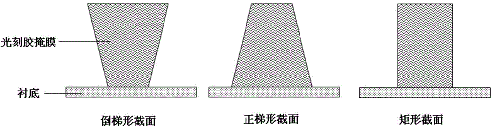
[0025] First of all, it should be noted that the etching mask set provided by the present invention is to form the required pattern on the surface of the substrate by using two photolithography processes. A mask set for etching is used, and then a required pattern is carved out of the mask set for etching by using a photolithography process.
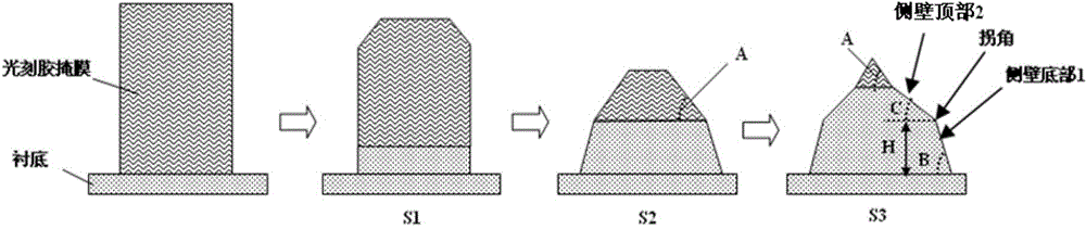
[0026] image 3 Two views of the cross-section and top view of the mask set for etching provided by the embodiment of the present invention. see image 3 , the mask set for etching includes a first mask layer 11 and a second mask layer 12, which are arranged sequentially from the surface of the substrate 10 from bottom to top, that is, the first ma...
PUM
 Abstract
Description
Claims
Application Information