[0061] In order to make the purpose, technical solutions and advantages of the embodiments of the present invention clearer, the technical solutions in the embodiments of the present invention will be clearly and completely described below in conjunction with the drawings in the embodiments of the present invention. Obviously, the described embodiments It is only some embodiments of the present invention, but not all embodiments. Based on the embodiments of the present invention, all other embodiments obtained by persons of ordinary skill in the art without making creative efforts belong to the protection scope of the present invention.
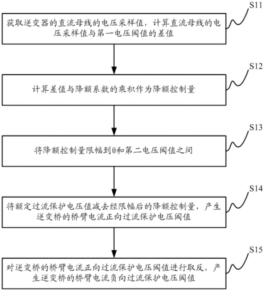
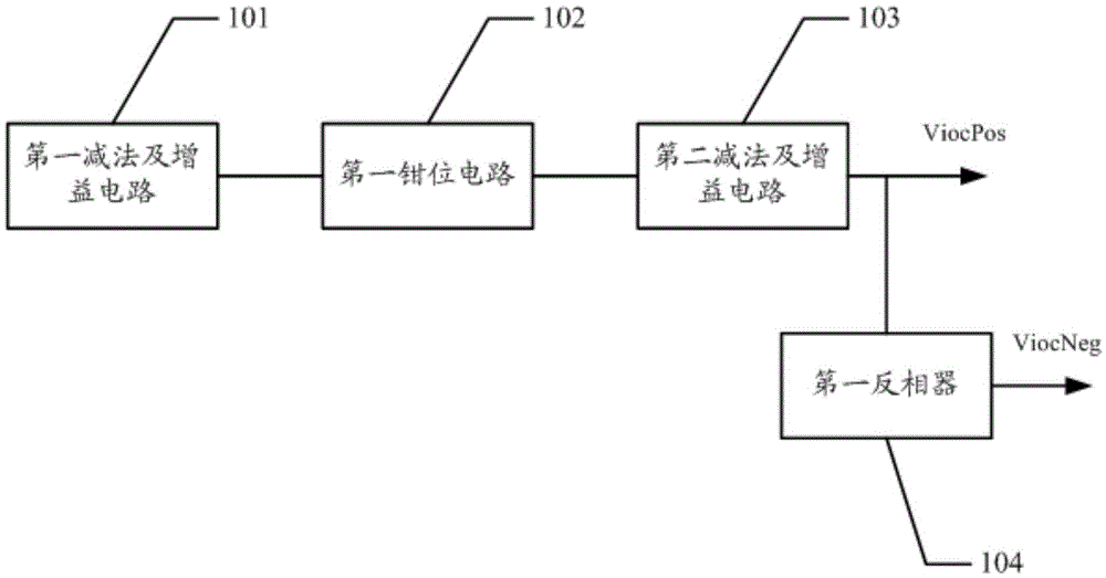
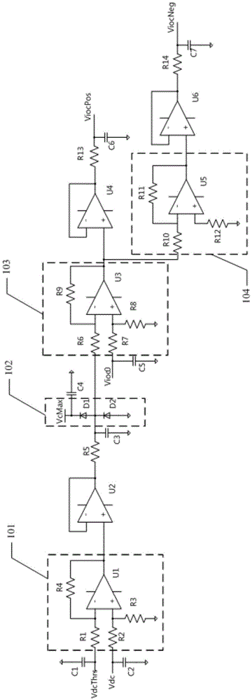
[0062] The invention discloses a method for adjusting the overcurrent protection threshold applied to an inverter, and dynamically adjusts the overcurrent protection threshold of the bridge arm in the inverter bridge according to the voltage of the DC bus of the inverter, thereby reducing the occurrence of switching tubes in the inverter The probability of damage due to overvoltage.
[0063] see figure 1 , figure 1 It is a flowchart of a method for adjusting an overcurrent protection threshold disclosed by the present invention. The method includes:
[0064] Step S11: Obtain the sampled voltage Vdc of the DC bus of the inverter, and calculate the difference between the sampled voltage Vdc of the DC bus and the first voltage threshold VdcThrs.
[0065] Wherein, the first voltage threshold VdcThrs is a voltage value corresponding to the derating threshold of the DC bus overcurrent protection.
[0066] Step S12: Calculate the product of the difference Vdc-VdcThrs and the derating coefficient K as the derating control amount.
[0067] Step S13: Limit the derating control amount to between 0 and the second voltage threshold VcMax.
[0068] Wherein, the second voltage threshold VcMax is a voltage value corresponding to the maximum overcurrent protection derating amount of the bridge arm current in the inverter bridge. The second voltage threshold VcMax should be configured as a value smaller than the rated overcurrent protection voltage Vioc0.
[0069] By executing step S13, when the DC bus voltage Vdc is lower than the first voltage threshold VdcThrs, no derating processing is performed on the bridge arm current positive overcurrent protection voltage threshold and the bridge arm current negative overcurrent protection voltage threshold of the inverter bridge, At the same time, prevent the situation that the output derating control amount is greater than the rated overcurrent protection voltage value Vioc0, that is, avoid the positive derating control amount of the bridge arm current and the negative derating control amount of the bridge arm current of the inverter bridge. value case.
[0070] Step S14: Subtracting the limited derating control amount from the rated overcurrent protection voltage value Vioc0 to generate a bridge arm current forward overcurrent protection voltage threshold ViocPos of the inverter bridge.
[0071] Wherein, the rated overcurrent protection voltage value Vioc0 is: the voltage value corresponding to the bridge arm overcurrent protection threshold of the inverter bridge when the DC bus voltage Vdc of the inverter is lower than the first voltage threshold VdcThrs. That is, the voltage value corresponding to the overcurrent protection threshold of the bridge arm of the inverter bridge under the normal operation state of the inverter.
[0072] Step S15: Negating the bridge arm current positive overcurrent protection voltage threshold ViocPos of the inverter bridge to generate the inverter bridge bridge arm current negative overcurrent protection voltage threshold ViocNeg.
[0073] Based on the method for adjusting the overcurrent protection threshold disclosed in the present invention, when the voltage sampling value of the DC bus of the inverter is higher than the set first voltage threshold, according to the difference between the voltage sampling value of the DC bus and the first voltage threshold value, dynamically derate the bridge arm current positive overcurrent protection voltage threshold and the bridge arm current negative overcurrent protection voltage threshold of the inverter bridge, thereby limiting the output current amplitude of the bridge arm in the inverter bridge and avoiding inverter The switching tubes in the bridge are subjected to high overvoltage during the switching action, which reduces the probability of the switching tubes being damaged.
[0074] In implementation, the first voltage threshold may be configured as an upper limit value of the DC bus voltage of the inverter in a state of continuously outputting rated power. Taking a photovoltaic inverter as an example, the first voltage threshold may be configured as a full-load MPPT (Maximum Power Point Tracking) voltage upper limit of the photovoltaic inverter.
[0075] The invention also discloses an overcurrent protection threshold adjustment circuit applied to inverters, please refer to figure 2 As shown, the overcurrent protection threshold adjustment circuit includes: a first subtraction and gain circuit 101 , a first clamping circuit 102 , a second subtraction and gain circuit 103 , and a first inverter 104 .
[0076] in:
[0077] The first subtraction and gain circuit 101 is used to calculate the difference between the voltage sampling value Vdc of the DC bus of the inverter and the first voltage threshold VdcThrs, and calculate the product of the difference Vdc-VdcThrs and the derating coefficient K as the derating control quantity. Wherein, the first voltage threshold is a voltage value corresponding to the derating threshold of the DC bus overcurrent protection.
[0078] The first clamping circuit 102 is connected to the output terminal of the first subtraction and gain circuit 101, and is used for limiting the derating control output output by the first subtraction and gain circuit 101 to be between 0 and the second voltage threshold VcMax. Wherein, the second voltage threshold VcMax is a voltage value corresponding to the maximum overcurrent protection derating amount of the bridge arm current in the inverter bridge.
[0079] One input terminal of the second subtraction and gain circuit 103 is connected with the first clamping circuit 102, and is used to subtract the derating control amount after the limit from the rated overcurrent protection voltage value Vioc0 to generate the bridge arm current of the inverter bridge Positive overcurrent protection voltage threshold ViocPos. Wherein, the gain of the second subtraction and gain circuit is 1.
[0080] The first inverter 104 is connected to the output end of the second subtraction and gain circuit 103, and is used to reverse the bridge arm current positive overcurrent protection voltage threshold ViocPos of the inverter bridge to generate the bridge arm current negative of the inverter bridge. To the overcurrent protection voltage threshold ViocNeg.
[0081] The overcurrent protection threshold adjustment circuit applied to the inverter disclosed above in the present invention, when the voltage of the DC bus of the inverter is higher than the set first voltage threshold, according to the voltage value of the DC bus and the first voltage threshold The difference between the bridge arm current positive overcurrent protection voltage threshold and the bridge arm current negative overcurrent protection voltage threshold of the inverter bridge is dynamically derated, so as to limit the output current amplitude of the bridge arm in the inverter bridge and avoid The switching tubes in the inverter bridge are subjected to excessive overvoltage during switching operations, reducing the probability of the switching tubes being damaged.
[0082] In implementation, the specific circuit structures of the first subtraction and gain circuit 101, the first clamping circuit 102, the second subtraction and gain circuit 103, and the first inverter 104 can be found in image 3 shown.
[0083] The first subtraction and gain circuit 101 includes a first resistor R1, a second resistor R2, a third resistor R3, a fourth resistor R4 and a first operational amplifier U1.
[0084] Wherein, the first terminal of the first resistor R1 is connected to the first voltage threshold VdcThrs, and the second terminal of the first resistor R1 is connected to the inverting input terminal of the first operational amplifier U1. The first end of the second resistor R2 is connected to the sampled voltage Vdc of the DC bus, and the second end of the second resistor R2 is connected to the non-inverting input end of the first operational amplifier U1. The third resistor R3 is connected between the non-inverting input terminal of the first operational amplifier U1 and the ground terminal. The fourth resistor R4 is connected between the inverting input terminal and the output terminal of the first operational amplifier U1. The output terminal of the first operational amplifier U1 is the output terminal of the first subtraction and gain circuit 101 .
[0085] If the first resistor R1 and the second resistor R2 are configured as resistors with a resistance value of r1, and the third resistor R3 and the fourth resistor R4 are configured as resistors with a resistance value of r2, then the derating coefficient K=r2/r1. The derating coefficient of the first subtraction and gain circuit 101 can be adjusted by adjusting the resistance values of the first resistor R1 , the second resistor R2 , the third resistor R3 and the fourth resistor R4 .
[0086] The first clamping circuit 102 includes a first diode D1 and a second diode D2.
[0087] Wherein, the cathode of the first diode D1 is connected to the second voltage threshold VcMax, the anode of the first diode D1 is connected to the cathode of the second diode D2, and the anode of the second diode D2 is grounded. The common terminal of the first diode D1 and the second diode D2 is connected to the output terminal of the first subtraction and gain circuit 101 , specifically to the output terminal of the first operational amplifier U1 .
[0088] The second subtraction and gain circuit 103 includes a sixth resistor R6, a seventh resistor R7, an eighth resistor R8, a ninth resistor R9 and a third operational amplifier U3.
[0089] Wherein, the first end of the sixth resistor R6 is connected to the first clamping circuit 102, specifically connected to the common end of the first diode D1 and the second diode D2, and the second end of the sixth resistor R6 is connected to the first clamping circuit 102. Three operational amplifiers connected to the inverting input of U3. The first terminal of the seventh resistor R7 is connected to the rated overcurrent protection voltage Vioc0, and the second terminal of the seventh resistor R7 is connected to the non-inverting input terminal of the third operational amplifier U3. The eighth resistor R8 is connected between the non-inverting input terminal of the third operational amplifier U3 and the ground terminal. The ninth resistor R9 is connected between the inverting input terminal and the output terminal of the third operational amplifier U3. The output terminal of the third operational amplifier U3 is the output terminal of the second subtraction and gain circuit 103 .
[0090]By configuring the sixth resistor R6 , the seventh resistor R7 , the eighth resistor R8 and the ninth resistor R9 as resistors with the same resistance value, the gain of the second subtraction and gain circuit 103 can be set to 1.
[0091] The first inverter 104 includes a tenth resistor R10, an eleventh resistor R11, a twelfth resistor R12 and a fifth operational amplifier U5.
[0092] Wherein, the first end of the tenth resistor R10 is connected to the output end of the second subtraction and gain circuit 103, specifically the output end of the third operational amplifier U3, and the second end of the tenth resistor R10 is connected to the fifth operational amplifier U5 The inverting input terminal connection. The eleventh resistor R11 is connected between the inverting input terminal and the output terminal of the fifth operational amplifier U5. The twelfth resistor R12 is connected between the non-inverting input terminal of the fifth operational amplifier U5 and the ground point. The output terminal of the fifth operational amplifier U5 is the output terminal of the first inverter 104 .
[0093] By configuring the tenth resistor R10 and the eleventh resistor R11 as resistors with the same resistance value, the gain of the first inverter 104 can be 1.
[0094] As a preferred implementation, a first voltage follower U2 can be further set in the overcurrent protection threshold adjustment circuit, such as image 3 As shown in , the input terminal of the first voltage follower U2 is connected to the output terminal of the first subtraction and gain circuit 101 , and the output terminal of the first voltage follower U2 is connected to the first clamping circuit 102 . The first voltage follower U2 can increase the input impedance and reduce the output impedance, so as to achieve impedance matching.
[0095] In addition, a second voltage follower U4 can be further set in the overcurrent protection threshold adjustment circuit, such as image 3 As shown in , the input end of the second voltage follower U4 is connected to the output end of the second subtraction and gain circuit 103 . The second voltage follower U4 can increase the input impedance and reduce the output impedance, so as to achieve impedance matching.
[0096] In addition, a third voltage follower U6 can be further set in the overcurrent protection threshold adjustment circuit, such as image 3 As shown in , the input terminal of the third voltage follower U6 is connected to the output terminal of the first inverter 104 . The third voltage follower U6 can increase the input impedance and reduce the output impedance, thereby realizing impedance matching.
[0097] In order to reduce the interference in the circuit, a first low-pass filter can be provided between the output terminal of the first voltage follower U2 and the first clamping circuit 102 . like image 3 As shown in , the first low-pass filter includes a fifth resistor R5 and a third capacitor C3.
[0098] In addition, a second low-pass filter may also be provided at the output terminal of the second voltage follower U4, and a third low-pass filter may be provided at the output terminal of the third voltage follower U6. like image 3 As shown in , the second low-pass filter includes a thirteenth resistor R13 and a sixth capacitor C6, and the third low-pass filter includes a fourteenth resistor R14 and a seventh capacitor C7.
[0099] exist image 3 In the overcurrent protection threshold adjustment circuit shown, the first filter capacitor C1 is connected to the first end of the first resistor R1, the first filter capacitor C2 is connected to the first end of the second resistor R2, and the first two-pole The cathode of the tube D1 is connected with a fourth filter capacitor C4.
[0100] The method for adjusting the over-current protection threshold and the over-current protection threshold adjustment circuit disclosed above in the present invention can be applied to inverters with any level value.
[0101] The present invention also discloses another method for adjusting the overcurrent protection threshold, which is applied to N-level inverters, where N is an odd number not less than 3, and the process is as follows Figure 4 shown, including:
[0102] Step S41: Obtain a sampled voltage value of the DC bus of the inverter, and calculate a first difference between the sampled voltage value of the DC bus and a first voltage threshold.
[0103] Wherein, the first voltage threshold is a voltage value corresponding to the derating threshold of the DC bus overcurrent protection.
[0104] Step S42: Calculate the product of the first difference and the first derating coefficient as the first derating control amount.
[0105] Step S43: Limit the first derating control amount to between 0 and the second voltage threshold.
[0106] Wherein, the second voltage threshold is a voltage value corresponding to the maximum overcurrent protection derating amount of the bridge arm current in the inverter bridge.
[0107] Step S44: Acquiring sampled voltage values of N−1 capacitors constituting the capacitor string in the inverter, and determining a maximum sampled voltage value among the sampled voltage values of the N−1 capacitors.
[0108] Taking a three-level inverter as an example, its capacitor string is composed of two capacitors in series, and taking a five-level inverter as an example, its capacitor string is composed of four capacitors in series. In step S14, it is necessary to obtain the voltage sample value of each capacitor in the capacitor string, the number of voltage sample values is N-1, and then determine the maximum voltage sample value among the N-1 voltage sample values.
[0109] Step S45: Calculate a second difference between the maximum voltage sample value and the third voltage threshold.
[0110] Wherein, the third voltage threshold is VdcThrs/(N-1), and VdcThrs is the first voltage threshold.
[0111] Step S46: Calculate the product of the second difference and the second derating coefficient as the second derating control amount.
[0112] Step S47: limiting the second derating control amount to be between 0 and the second voltage threshold.
[0113] Step S48: Determine the maximum value of the limited first derating control amount and the limited second derating control amount.
[0114] Step S49: subtracting the maximum value from the rated overcurrent protection voltage value to generate a bridge arm current forward overcurrent protection voltage threshold of the inverter bridge.
[0115] Step S410 : Inverting the positive overcurrent protection voltage value of the bridge arm current of the inverter bridge to generate a negative overcurrent protection voltage threshold of the bridge arm current of the inverter bridge.
[0116] Based on the method for adjusting the overcurrent protection threshold disclosed in the present invention, when the voltage sampling value of the DC bus of the inverter is higher than the set first voltage threshold, or the voltage sampling value at both ends of any capacitor in the capacitor string is higher than When the third voltage threshold is set, determine the first difference between the voltage sampling value of the DC bus and the first voltage threshold, determine the second difference between the maximum sampling voltage value of the capacitor and the second voltage threshold, and then use the first The larger difference between the difference and the second difference will dynamically derate the positive overcurrent protection voltage threshold of the bridge arm current and the negative overcurrent protection voltage threshold of the bridge arm current of the inverter bridge, thereby limiting the inverter The output current amplitude of the bridge arm in the bridge prevents the switching tubes in the inverter bridge from being subjected to excessive overvoltage during switching operations, and reduces the probability of the switching tubes being damaged. At the same time, in the process of adjusting the overcurrent protection threshold, the voltage sampling value of each capacitor in the capacitor string is integrated for dynamic derating, which can eliminate the voltage stress deviation of the switch tube caused by the offset of each capacitor relative to the midpoint.
[0117] In implementation, the first voltage threshold may be configured as an upper limit value of the DC bus voltage of the inverter in a state of continuously outputting rated power. Taking a photovoltaic inverter as an example, the first voltage threshold may be configured as a full-load MPPT (Maximum Power Point Tracking) voltage upper limit of the photovoltaic inverter.
[0118] The invention also discloses an overcurrent protection threshold adjustment circuit applied to an N-level inverter, wherein N is an odd number not less than 3. The structure of the overcurrent protection threshold adjustment circuit is as follows Figure 5 As shown, it includes a third subtraction and gain circuit 201, a second clamping circuit 202, a first comparison circuit 203, a fourth subtraction and gain circuit 204, a third clamping circuit 205, a second comparison circuit 206, the fifth subtraction and a gain circuit 207 , and a second inverter 208 .
[0119] in:
[0120] The third subtraction and gain circuit 201 is used to calculate the first difference between the voltage sampling value of the DC bus of the inverter and the first voltage threshold, and calculate the product of the first difference and the first derating factor as the first derating Control amount. Wherein, the first voltage threshold is a voltage value corresponding to the derating threshold of the DC bus overcurrent protection.
[0121] The second clamping circuit 202 is connected to the output terminal of the third subtraction and gain circuit 201, and is used for limiting the first derating control amount to be between 0 and the second voltage threshold. Wherein, the second voltage threshold is a voltage value corresponding to the maximum overcurrent protection derating amount of the bridge arm current in the inverter bridge.
[0122] The first comparison circuit 203 is used for comparing the voltage sample values of the N−1 capacitors constituting the capacitor string in the inverter, and determining the maximum voltage sample value among the voltage sample values of the N−1 capacitors.
[0123] An input terminal of the fourth subtraction and gain circuit 204 is connected to the output terminal of the first comparison circuit 203, and is used to calculate the second difference between the maximum voltage sampling value and the third voltage threshold, and calculate the second difference and the second drop The product of the rating coefficient is used as the second derating control amount.
[0124] Wherein, the third voltage threshold is VdcThrs/(N-1), and VdcThrs is the first voltage threshold.
[0125] The third clamping circuit 205 is connected to the output terminal of the fourth subtraction and gain circuit 204, and is used for reducing the second derating control amount to between 0 and the second voltage threshold.
[0126] One input terminal of the second comparison circuit 206 is connected to the second clamping circuit 202, and the other input terminal is connected to the third clamping circuit 205, for determining the first derating control amount after limiting and the first derating control amount after limiting. The maximum value of the second derating control amount.
[0127] One input terminal of the fifth subtraction and gain circuit 207 is connected to the output terminal of the second comparison circuit 206, and is used to subtract the maximum value from the rated overcurrent protection voltage value to generate the bridge arm current forward overcurrent protection voltage of the inverter bridge threshold. Wherein, the gain of the fifth subtraction and gain circuit 207 is 1.
[0128] The second inverter 208 is connected to the output end of the fifth subtraction and gain circuit 207, and is used to reverse the positive overcurrent protection voltage value of the bridge arm current of the inverter bridge to generate the negative direction of the bridge arm current of the inverter bridge. Overcurrent protection voltage threshold.
[0129] In the overcurrent protection threshold adjustment circuit applied to N-level inverters disclosed above in the present invention, when the voltage sampling value of the DC bus of the inverter is higher than the set first voltage threshold, or any one of the capacitor strings When the voltage sampling value at both ends of the capacitor is higher than the set third voltage threshold, determine the first difference between the voltage sampling value of the DC bus and the first voltage threshold, and determine the first difference between the maximum sampling voltage value of the capacitor and the second voltage threshold Two differences, and then use the larger difference between the first difference and the second difference to check the positive overcurrent protection voltage threshold of the bridge arm current and the negative overcurrent protection voltage threshold of the bridge arm current of the inverter bridge. Dynamic derating, so as to limit the output current amplitude of the bridge arm in the inverter bridge, avoid the switch tube in the inverter bridge from being subjected to excessive overvoltage during switching, and reduce the probability of the switch tube being damaged. At the same time, in the process of adjusting the overcurrent protection threshold, the voltage sampling value of each capacitor in the capacitor string is integrated for dynamic derating, which can eliminate the voltage stress deviation of the switch tube caused by the offset of each capacitor relative to the midpoint.
[0130] Each embodiment in this specification is described in a progressive manner, each embodiment focuses on the difference from other embodiments, and the same and similar parts of each embodiment can be referred to each other.
[0131]The above description of the disclosed embodiments is provided to enable any person skilled in the art to make or use the invention. Various modifications to these embodiments will be readily apparent to those skilled in the art, and the general principles defined herein may be implemented in other embodiments without departing from the spirit or scope of the invention. Therefore, the present invention will not be limited to the embodiments shown herein, but is to be accorded the widest scope consistent with the principles and novel features disclosed herein.