

Universality efficient synchrotron radiation visual representation method of crystal microstructure
A microstructure and universal technology, applied in the field, can solve the problems of cumbersome and time-consuming, and achieve the effect of high application value, improved processing speed, and simple data processing.
- Summary
- Abstract
- Description
- Claims
- Application Information
AI Technical Summary
Problems solved by technology
Method used
Image

Examples
Embodiment Construction
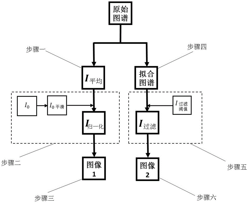
[0055] In order to make the above-mentioned purposes, features and advantages of the present invention more obvious and understandable, the following in conjunction with the attached figure 2 The example samples shown illustrate in detail the specific implementation of the present invention.
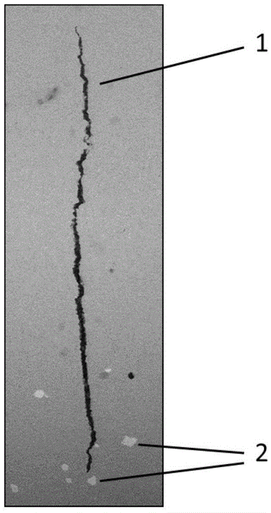
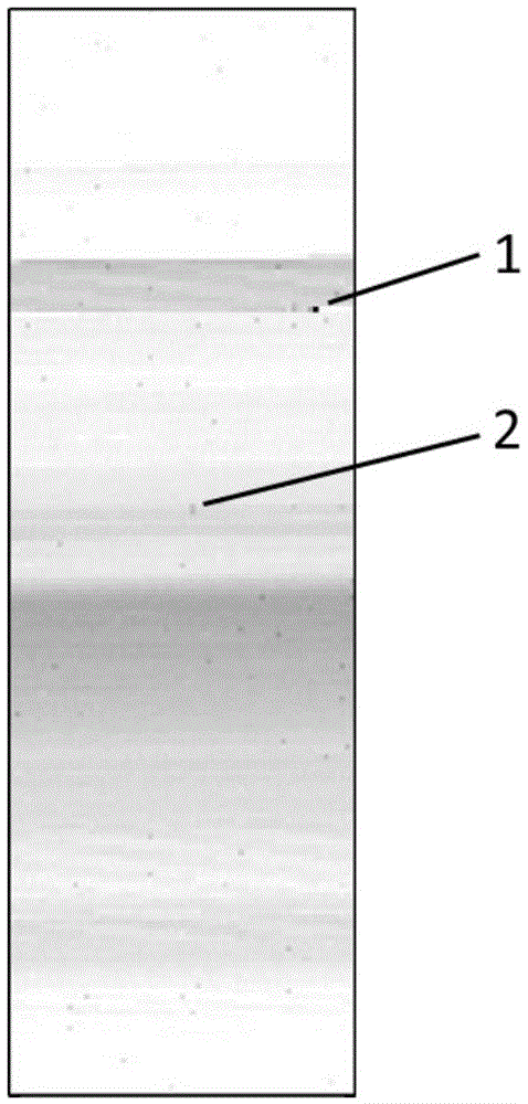
[0056] attached figure 2 The example sample shown is the sample prepared by 3D printing technology, in the attached figure 2 In the backscattered electron imaging image used, it can be seen that there are microcracks 1 and several precipitated phases 2 in the sample area.
[0057] Step 1: The value obtained by each normal pixel point of the detector in the original spectrum obtained by the known synchrotron radiation micro-area Laue diffraction experiment on the sample of the embodiment is averaged to obtain the mean value I 平均 (x,y). Wherein, the detector error pixel includes the detector dead pixel and the seam of the detection original that compose the detector. Because the int...
PUM
 Abstract
Description
Claims
Application Information