Array substrate and manufacturing method thereof
An array substrate and substrate substrate technology, which is applied in the manufacture of semiconductor/solid-state devices, semiconductor/solid-state device components, semiconductor devices, etc. The effect of reducing the risk of cracking, enhancing mechanical strength, and strong process compatibility
- Summary
- Abstract
- Description
- Claims
- Application Information
AI Technical Summary
Problems solved by technology
Method used
Image

Examples
Embodiment Construction
[0032] Embodiments of the present invention will be described in detail below with reference to the accompanying drawings, wherein like reference numerals correspond to like elements. However, the present invention has many different embodiments, and it should not be construed as limiting the present invention to the described embodiments; but only by providing the embodiments of the present invention, so that the present disclosure will be comprehensive and complete, and will fully inform those skilled in the art. to convey the concept of the invention.
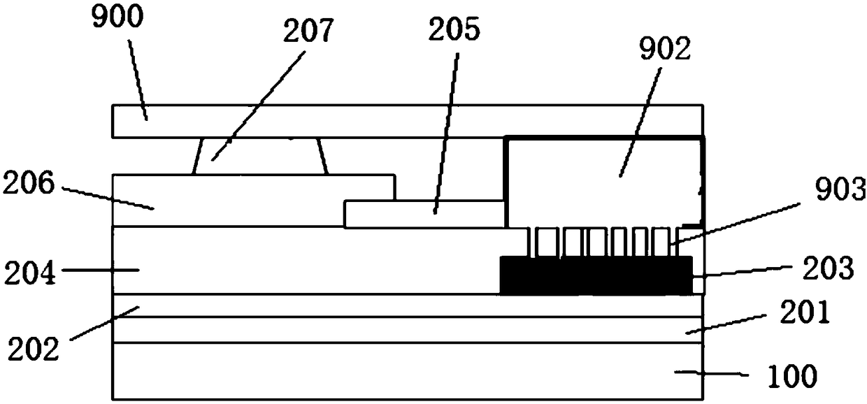
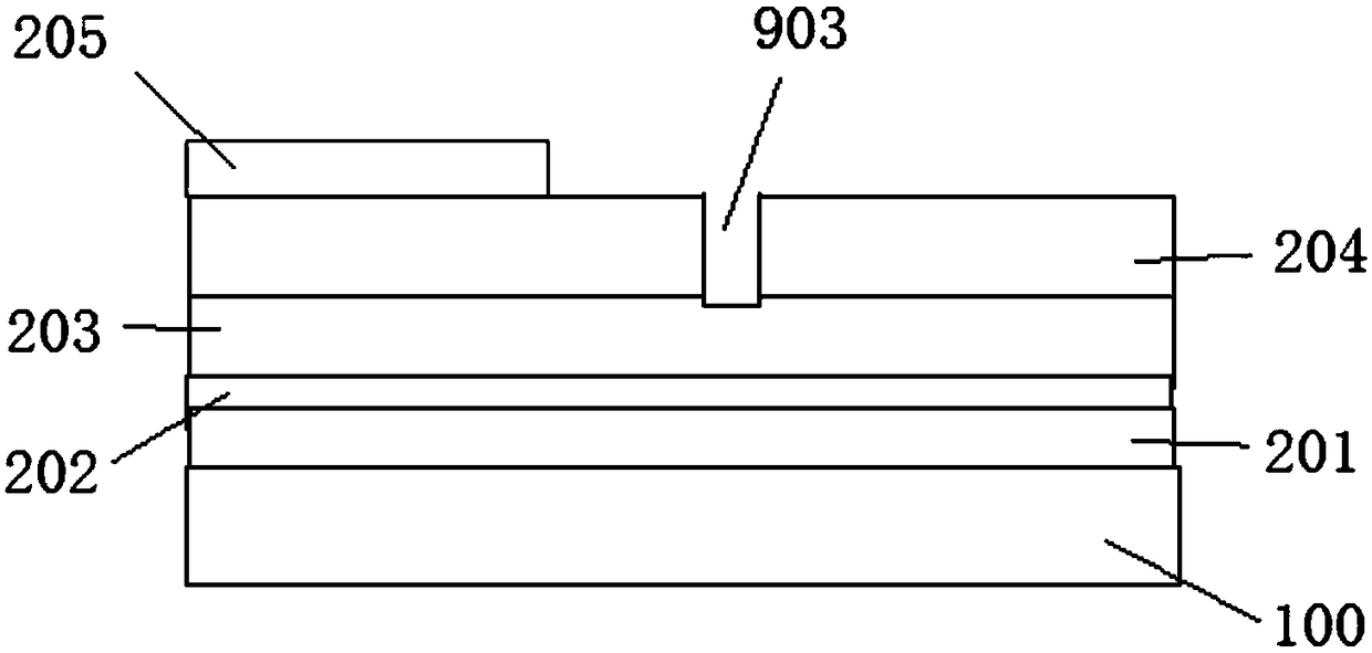
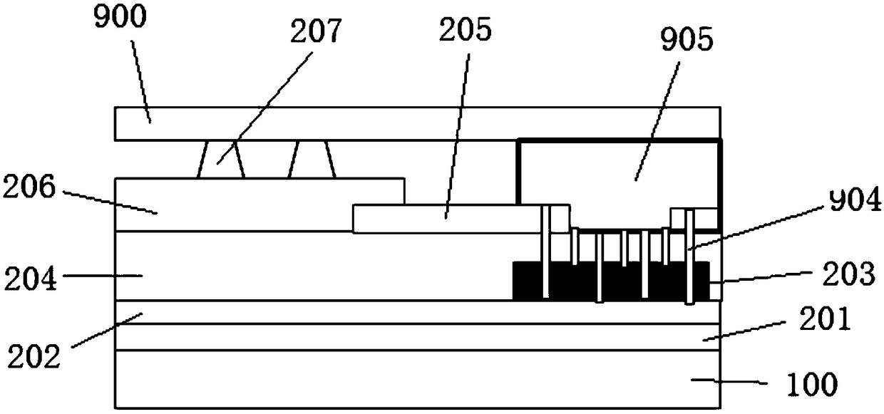
[0033] image 3 An embodiment of the array substrate provided according to the present invention is shown, which includes: a display area and a packaging area, the packaging area includes multiple functional layers, and the packaging area includes: a through hole 904, the through hole Through at least one functional layer, the encapsulation glue flows in through the through hole; the groove 905 is arranged above at least pa...
PUM
 Abstract
Description
Claims
Application Information
 - R&D Engineer
- R&D Manager
- IP Professional
- Industry Leading Data Capabilities
- Powerful AI technology
- Patent DNA Extraction
Browse by: Latest US Patents, China's latest patents, Technical Efficacy Thesaurus, Application Domain, Technology Topic.
© 2024 PatSnap. All rights reserved.Legal|Privacy policy|Modern Slavery Act Transparency Statement|Sitemap