Electroluminescent device, manufacturing method thereof and display device

An electroluminescent device and a manufacturing method technology, applied in the direction of electric solid-state devices, semiconductor/solid-state device manufacturing, electrical components, etc., can solve the problems of different electron mobility and hole mobility, and the limitation of hole transport layer material selection, etc. Achieve the effect of reducing production cost and ensuring luminous efficiency

Active Publication Date: 2016-06-15
BOE TECH GRP CO LTD
View PDF8 Cites 26 Cited by
  • Summary
  • Abstract
  • Description
  • Claims
  • Application Information

AI Technical Summary

Problems solved by technology

[0004] The present invention provides an electroluminescence device, its manufacturing method, and a display device, which are used to solve the problem that the material selection of the hole transport layer is limited when the electron mobility of the electron transport layer is different from the hole mobility of the hole transport layer. The problem

Method used


Image

  • Electroluminescent device, manufacturing method thereof and display device
  • Electroluminescent device, manufacturing method thereof and display device

Examples


Embodiment 1

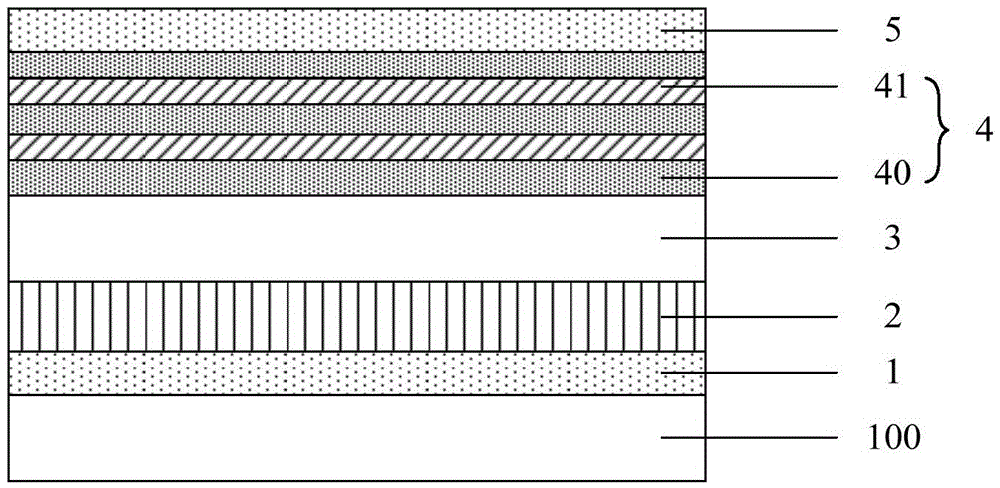
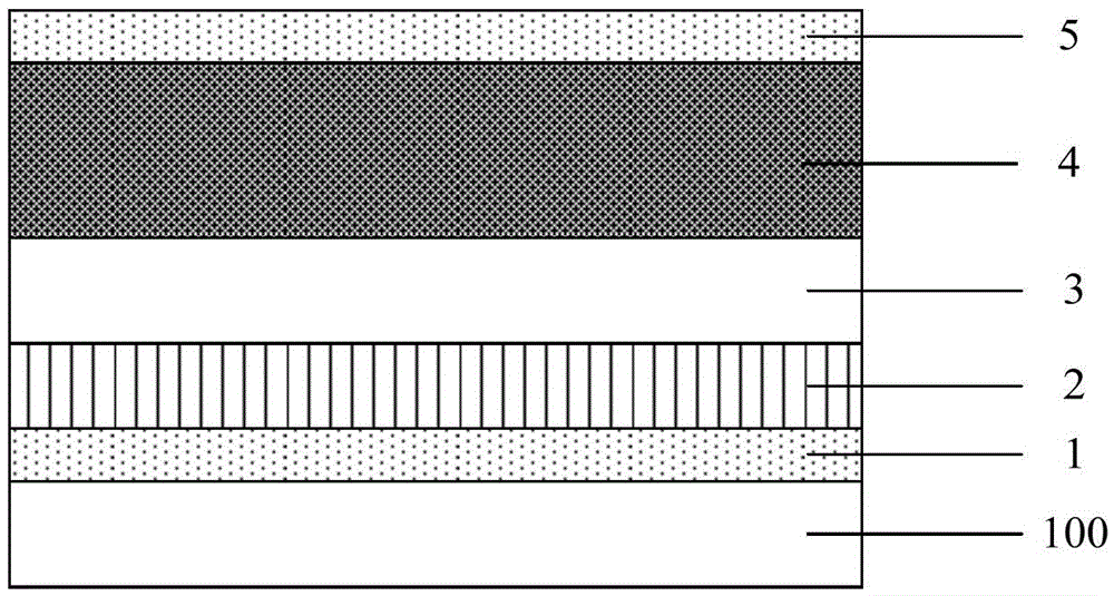
[0017] In this embodiment, an electroluminescent device is provided, comprising an anode 1 , a hole transport layer 2 , a light emitting layer 3 , an electron transport layer 4 and a cathode 5 sequentially arranged on a substrate 100 . The luminescent layer 3 is made of electroluminescent materials such as quantum dot materials and organic luminescent materials, and the recombination of electrons and holes in the luminescent layer 3 can excite the luminescent layer 3 to emit light. In order to improve luminous efficiency, a hole injection layer (not shown) can also be set between the anode 1 and the hole transport layer 2, and an electron injection layer (not shown) can be set between the electron transport layer 4 and the cathode 5. out).

[0018] The electron transport layer 4 includes a first film layer for transporting electrons, and also includes an adjustment structure arranged in contact with the first film layer, and the adjustment structure is used for adjusting the e...

Embodiment 2

[0033] Based on the same inventive concept, this embodiment provides a method for manufacturing the electroluminescent device in Embodiment 1, including:

[0034] An anode, a hole transport layer, a light emitting layer, an electron transport layer and a cathode are sequentially formed on a substrate. The light-emitting layer can be made of quantum dot materials, such as CdSe / ZnS, CdS / ZnS and other core-shell structure quantum dots, or can be made of organic light-emitting materials such as fluorescent materials and phosphorescent materials. In order to improve luminous efficiency, a hole injection layer may be formed between the anode and the hole transport layer, and an electron injection layer may be formed between the electron transport layer and the cathode.

[0035] Wherein, the step of forming electron transport layer comprises:

[0036] A first film layer for transporting electrons is formed.

[0037] An adjustment structure disposed in contact with the first film la...


PUM


Abstract

The invention relates to the technical field of display and discloses an electroluminescent device, a manufacturing method thereof and a display device. An electron transmission layer of the electroluminescent device comprises a first film layer used for transmitting electrons and an adjusting structure in contact with the first film layer. The adjusting structure is used for adjusting the electron mobility of the electron transmission layer so as to realize matching of the electron mobility with the cavity mobility of a cavity transmission layer, so that the selection of the material of the cavity transmission layer is not limited, the production cost is lowered, and the luminescence efficiency of the device is ensured.

Description

technical field [0001] The invention relates to the field of display technology, in particular to an electroluminescence device, a manufacturing method thereof, and a display device. Background technique [0002] As a zero-dimensional nanomaterial, quantum dot material has adjustable band gap, large specific surface area, and superior photoelectric performance. In recent years, it has attracted extensive attention in the fields of light-emitting diodes, solar cells, photodetectors, and displays. Especially in the field of display, electroluminescent quantum dot devices have achieved high luminous efficiency, and industrialization has gradually progressed. [0003] For electroluminescent quantum dot devices, taking CdSe / ZnS, CdS / ZnS and other core-shell structure quantum dot luminescent materials as examples, the currently widely used device structure is anode / hole injection layer / hole transport layer / quantum dot luminescence layer / electron transport layer / cathode. The elec...

Claims


Application Information

Patent Timeline
Patent Type & Authority Applications(China)
IPC IPC(8): H01L51/50
CPCH10K50/165H10K50/166H10K50/16H10K50/115H10K50/00H10K50/18H10K2102/331H10K50/167H10K2101/30H10K2102/00H10K2102/351
Inventor 孟虎
Owner BOE TECH GRP CO LTD
Why Eureka
Try Eureka