Transparent electroconductive film preparation method

A transparent conductive film and substrate technology, applied in circuits, electrical components, semiconductor devices, etc., can solve the problems affecting the luminous efficiency of LED chips and the high cost of the transparent conductive layer, and achieve the effect of convenient implementation, low cost and low environmental requirements.

Inactive Publication Date: 2015-09-30
HC SEMITEK SUZHOU
View PDF6 Cites 5 Cited by
  • Summary
  • Abstract
  • Description
  • Claims
  • Application Information

AI Technical Summary

Problems solved by technology

[0004] In order to solve the problems of the high cost of the transparent conductive layer and the influence on the luminous efficiency of the LED chip in the prior art, the embodiment of the present invention provides a method for preparing a transparent conductive film

Method used


Image

  • Transparent electroconductive film preparation method
  • Transparent electroconductive film preparation method
  • Transparent electroconductive film preparation method

Examples


Embodiment Construction

[0037] In order to make the object, technical solution and advantages of the present invention clearer, the implementation manner of the present invention will be further described in detail below in conjunction with the accompanying drawings.

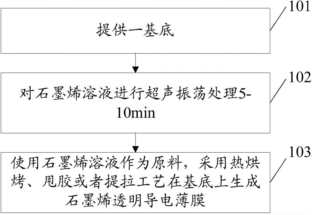
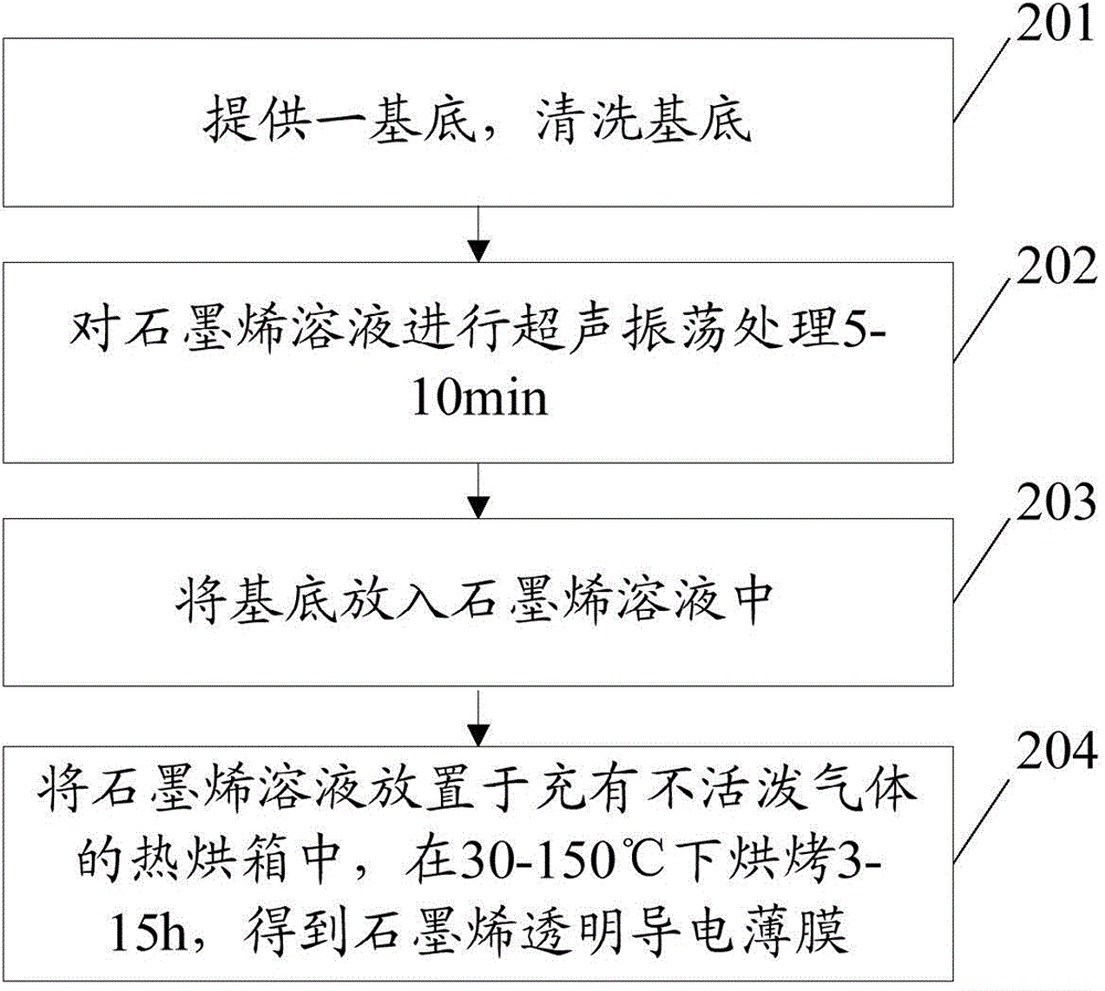
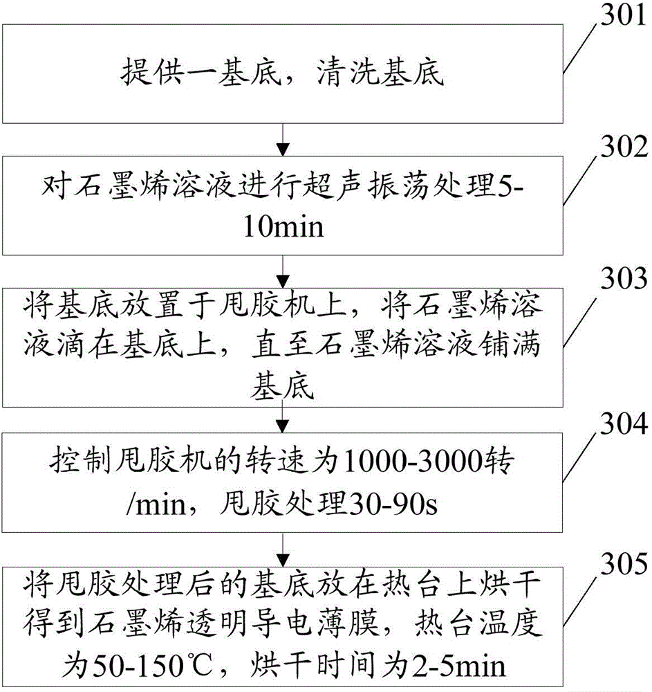
[0038] figure 1 A flow chart of a preparation method for a transparent conductive film is provided, see figure 1 , the method includes:

[0039] Step 101: Provide a base.

[0040] The substrate includes, but is not limited to, an LED epitaxial wafer.

[0041] Step 102: ultrasonically oscillating the graphene solution for 5-10 minutes, wherein the concentration of the graphene solution is 1-10 mg / L.

[0042] In the embodiment of the present invention, the graphene solution includes but is not limited to commercial graphene alcohol solution.

[0043] The use of 1-10mg / L graphene solution can ensure that the final graphene transparent conductive film can be at least a single layer, but the number of layers will not be too many, result...


PUM

PropertyMeasurementUnit
concentrationaaaaaaaaaa

Abstract

The invention discloses a transparent electroconductive film preparation method and belongs to the field of light-emitting diodes. The method includes: providing a substrate; subjecting a graphene solution to ultrasonic oscillation treatment for 5-10 minutes, wherein the concentration of the graphene solution is 1-10mg / L; using the graphene solution as a raw material, and generating the transparent graphene electroconductive film on the substrate by a heat baking technology, a whirl coating technology or a dip coating technology. The transparent electroconductive film preparation method has the advantages that the graphene solution is used as the raw material during preparation, thereby being lower than ITO (indium tin oxide) in cost; the transparent graphene electroconductive film is prepared by the heat baking technology, whirl coating technology or dip coating technology, and accordingly, the method is simple in used equipment, low in requirement on environments such as temperature and pressure and low in processing cost; the transparent graphene electroconductive film cannot absorb photons released by an active region, so that light-emitting efficiency of an LED chip is guaranteed.

Description

technical field [0001] The invention relates to the field of light emitting diodes, in particular to a preparation method of a transparent conductive film. Background technique [0002] The transparent conductive layer not only has high electrical conductivity, but also has high transmittance in a specific band of visible light, and is an important component of components such as LED (Light Emitting Diode, light emitting diode). At present, the widely used material for the transparent conductive layer is ITO (Indium Tin Oxides, indium tin oxide). [0003] However, since the In element in ITO is a rare metal element and is expensive, the material cost of the LED chip will be higher as a material for the transparent conductive layer; at the same time, when using ITO to prepare the transparent conductive layer, vacuum evaporation, chemical vapor phase, etc. are mainly used. deposition, pulsed laser deposition, and magnetron sputtering, etc., have high requirements for equipmen...

Claims


Application Information

Patent Timeline
Patent Type & Authority Applications(China)
IPC IPC(8): H01L33/42
CPCH01L33/42H01L2933/0016
Inventor 王群郭炳磊董彬忠李鹏王江波
Owner HC SEMITEK SUZHOU
Why Eureka
Try Eureka