

LED (Light-Emitting Diode) epitaxial structure and preparation method thereof
A technology of epitaxial structure and light shielding layer, applied in electrical components, circuits, semiconductor devices, etc., can solve the problem of light damage of quantum well layer, and achieve the effect of stable performance, good shielding effect and high melting point
- Summary
- Abstract
- Description
- Claims
- Application Information
AI Technical Summary
Problems solved by technology
Method used
Image

Examples
Embodiment Construction
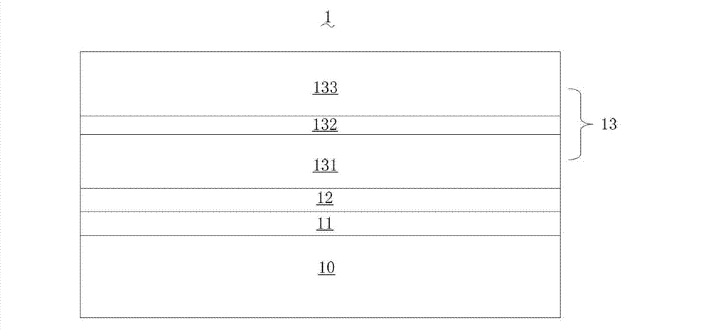
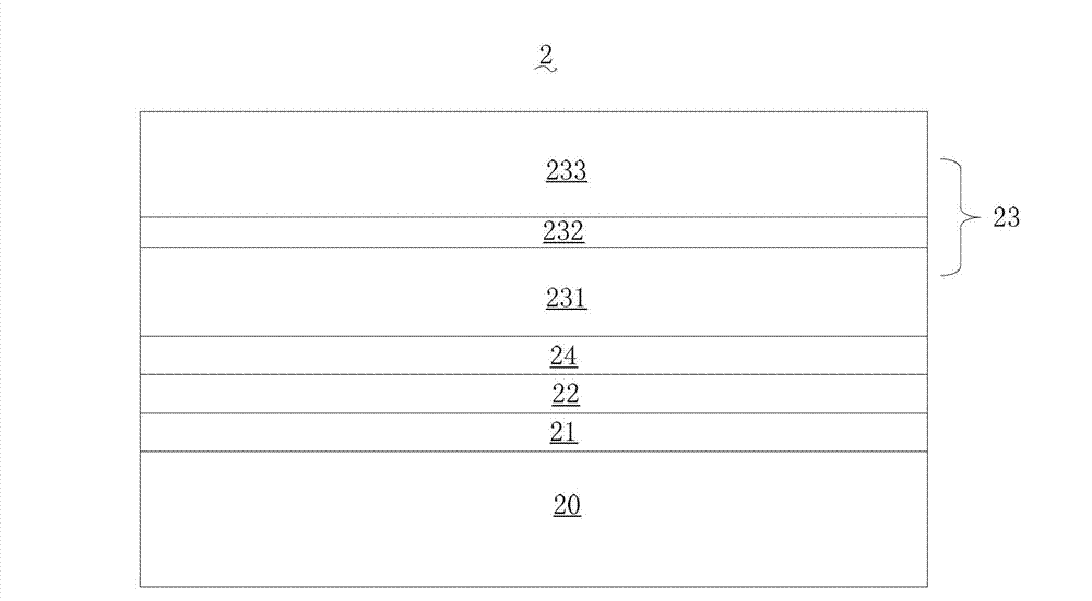
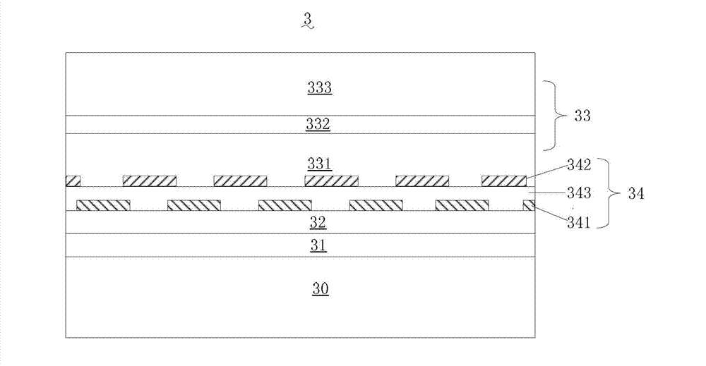
[0056] In the LED epitaxial structure of the prior art, a buffer layer, a sacrificial layer, an N-type GaN layer, a quantum well layer, and a P-type GaN layer are sequentially grown on the substrate, but when the substrate is lifted off by laser , the laser light will pass through the buffer layer, the sacrificial layer and the N-type gallium nitride layer and cause damage to the quantum well layer. After in-depth research on the prior art LED epitaxial structure, the inventor found that the absorption efficiency of the buffer layer, the sacrificial layer and the N-type gallium nitride layer to the laser light is low, which causes the laser light to pass through the buffer layer, the sacrificial layer and the N-type gallium nitride layer. Gallium nitride layer, when a light-shielding layer is prepared between the sacrificial layer and the quantum well layer, the absorption rate of the light-shielding layer for the laser light used to lift off the substrate is greater than that ...
PUM
 Abstract
Description
Claims
Application Information