

Polishing head leveling device and method
A leveling device and polishing head technology, applied in grinding devices, grinding machine tools, metal processing equipment, etc., can solve the problems of small wafer size, high cost, large volume of the leveling device, etc., to eliminate thread gaps and improve verticality. degree, improve the effect of leveling accuracy
- Summary
- Abstract
- Description
- Claims
- Application Information
AI Technical Summary
Problems solved by technology
Method used
Image

Examples
Embodiment Construction
[0026] The present invention will be further described below in conjunction with the accompanying drawings and specific embodiments.
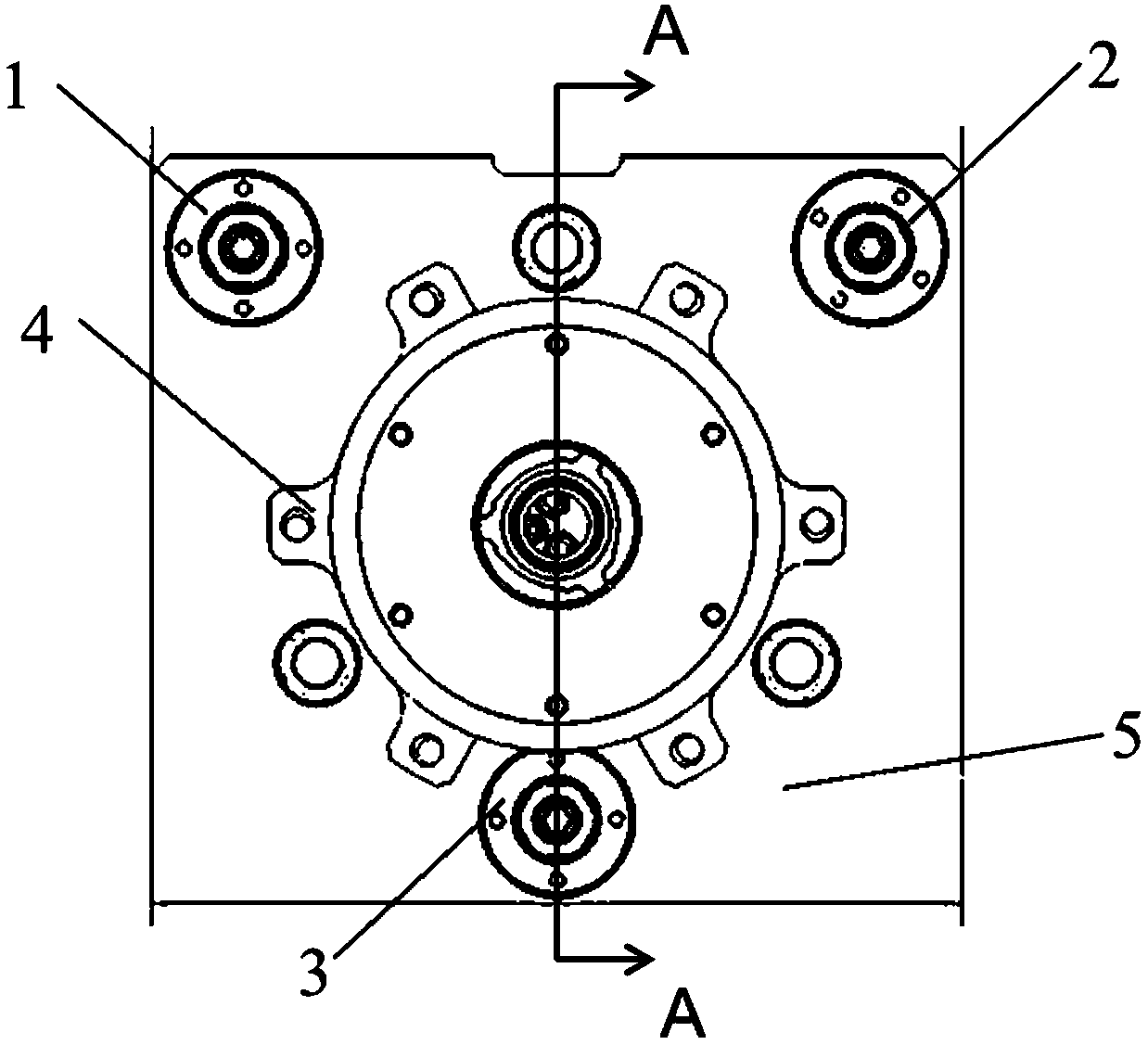
[0027] Such as Figure 1-3 As shown, under the adjustment of the first leveling screw group 1, the second leveling screw group 2 and the third leveling screw group 3, the adjustment plate 5 determines a plane according to three points, such as the first leveling screw The position of group 1 is fixed, the height of the second leveling screw group 2 makes the first leveling screw group 1 and the second leveling screw group 2 in a horizontal state; the height of the third leveling screw group 3 makes The first leveling screw group 1 and the third leveling screw group 3 are in a horizontal state; when the first leveling screw group 1, the second leveling screw group 2 and the third leveling screw group 3 are rigidly connected to each other , then the adjustment plate 5 is in a horizontal state at this moment.
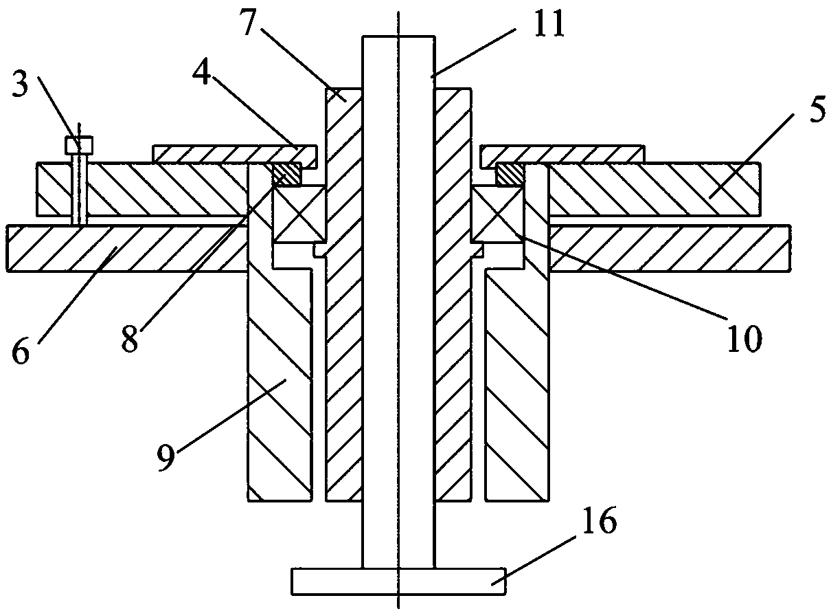
[0028] The adjusting plate 5 is pl...
PUM
 Abstract
Description
Claims
Application Information