Wiring board with dual wiring structures integrated together and method of making the same

A technology of wiring structure and manufacturing method, applied in the direction of printed circuit manufacturing, circuits, printed circuits, etc., can solve problems such as no fan-out routing, inability to solve characteristic problems, etc.

Inactive Publication Date: 2016-06-22
BRIDGE SEMICON
View PDF8 Cites 6 Cited by
  • Summary
  • Abstract
  • Description
  • Claims
  • Application Information

AI Technical Summary

Problems solved by technology

However, although these circuit boards can reduce inductance, they cannot solve other characteristic problems because they do not have sufficient fan-out routing capabilities to meet the high requirements of ultra-dense pitch flip-chip assemblies. (e.g. design flexibility)

Method used


Image

  • Wiring board with dual wiring structures integrated together and method of making the same
  • Wiring board with dual wiring structures integrated together and method of making the same
  • Wiring board with dual wiring structures integrated together and method of making the same

Examples


Embodiment 1

[0064] Figure 1-17 It is a diagram of a method for manufacturing a circuit board in an implementation aspect of the present invention, which includes a strengthening layer, a first wiring structure and a second wiring structure.

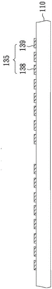
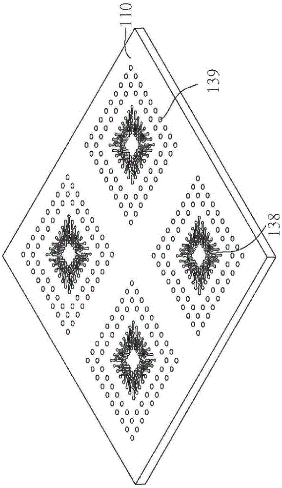
[0065] figure 1 and 2 They are respectively a cross-sectional view and a top perspective view of the routing circuit 135 formed on the sacrificial carrier 110 , wherein the routing circuit 135 is formed by metal deposition and metal patterning processes. In this figure, the sacrificial carrier 110 is a single-layer structure, and the routing circuit 135 includes bonding pads 138 and bonding pads 139 . The sacrificial carrier 110 is typically made of copper, aluminum, iron, nickel, tin, stainless steel, silicon or other metals or alloys, but any other conductive or non-conductive material can also be used. The thickness of the sacrificial carrier 110 is preferably in the range of 0.1 to 2.0 mm. In this embodiment, the sacrificial carrier 110 is m...

Embodiment 2

[0089] Figure 20-28 In another implementation aspect of the present invention, it is a diagram of a method for manufacturing a circuit board with a bending-resistant control member.

[0090] For the purpose of brief description, any descriptions in the above-mentioned embodiment 1 that can be used for the same application are incorporated here, and it is not necessary to repeat the same descriptions.

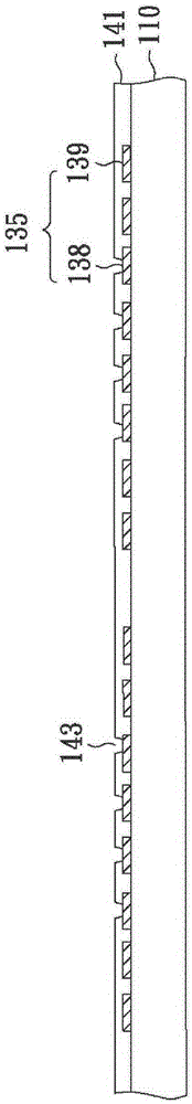
[0091] Figure 20 It is a cross-sectional view of the subassembly 10 and the reinforcing layer 20 placed on the third insulating layer 441 / metal layer 44 . Subassembly 10 with Figure 10 The structures shown are similar, and the only difference is that the sacrificial carrier 110 in this embodiment is a double-layer structure. In this figure, the third insulating layer 441 is interposed between the subassembly 10 and the metal layer 44 and between the reinforcement layer 20 and the metal layer 44, and the third insulation layer 441 contacts the second wire 155 of the subass...

Embodiment 3

[0104] Figure 30 It is a cross-sectional view of the circuit board 300 according to another embodiment of the present invention, in which the second wiring structure 420 is further electrically coupled to the strengthening layer 20 for ground connection.

[0105] In this embodiment, the circuit board 300 is prepared by a process similar to that described in Embodiment 2, the only difference is that there is no bonding pad on the first surface 101 of the first wiring structure 120 in this embodiment, and the second There is no positioning element formed on the wiring structure 420 , while the third wire 445 of the second wiring structure 420 is in direct contact with the strengthening layer 20 through the additional third conductive blind hole 448 , so as to be further electrically coupled to the metal-containing strengthening layer 20 .

[0106] Figure 31 is a cross-sectional view of a semiconductor assembly, wherein a semiconductor element 57 shown as a 3D stacked chip is ...


PUM


Abstract

A wiring board with integrated dual wiring structures is characterized in that first and second wiring structures are positioned within and beyond a through opening of a stiffener, respectively. The mechanical robustness of the stiffener can prevent the wiring board from warping. The first wiring structure, positioned within the through opening of the stiffener, can provide primary fan-out routing, whereas the second wiring structure not only provides further fan-out wiring structure for the first wiring structure, but also mechanically binds the first wiring structure with the stiffener.

Description

technical field [0001] The invention relates to a circuit board, in particular to a circuit board which integrates a double wiring structure inside and outside the through opening of the strengthening layer and its manufacturing method. Background technique [0002] The market trend of electronic devices (such as multimedia devices) tends to require faster and thinner designs. One of the methods is to interconnect semiconductor chips through a core-less substrate, which enables thinner combined devices and improves signal integrity. US Patent Nos. 7,851,269, 7,902,660, 7,981,728 and 8,227,703 disclose various coreless substrates based on this purpose. However, although these circuit boards can reduce inductance, they cannot solve other characteristic problems because they do not have sufficient fan-out routing capabilities to meet the high requirements of ultra-dense pitch flip-chip assemblies. (e.g. design flexibility). [0003] For the above reasons and other reasons de...

Claims


Application Information

Patent Timeline
Patent Type & Authority Applications(China)
IPC IPC(8): H01L23/485H01L21/60
CPCH01L23/49816H01L23/49822H01L23/49827H01L23/562H01L2224/16225H01L2224/73204H05K1/181H05K1/183H05K3/4682H05K3/4694H01L25/065Y02P70/50
Inventor 林文强王家忠
Owner BRIDGE SEMICON
Why Eureka
Try Eureka