Circuit board with double reinforcement layer and integrated dual routing circuit and its manufacturing method
A manufacturing method and reinforcement layer technology, applied in the direction of circuits, printed circuit components, printed circuit stress/deformation reduction, etc., can solve problems such as inability to solve characteristic problems, no fan-out routing, etc.
- Summary
- Abstract
- Description
- Claims
- Application Information
AI Technical Summary
Problems solved by technology
Method used
Image
Examples
Embodiment 1
[0055] Figure 1-Figure 18 In the first embodiment of the present invention, a manufacturing method diagram of a circuit board, which includes a first reinforcement layer, a first routing circuit, a second routing circuit, a series of vertical connection vias and a second reinforcement layer .
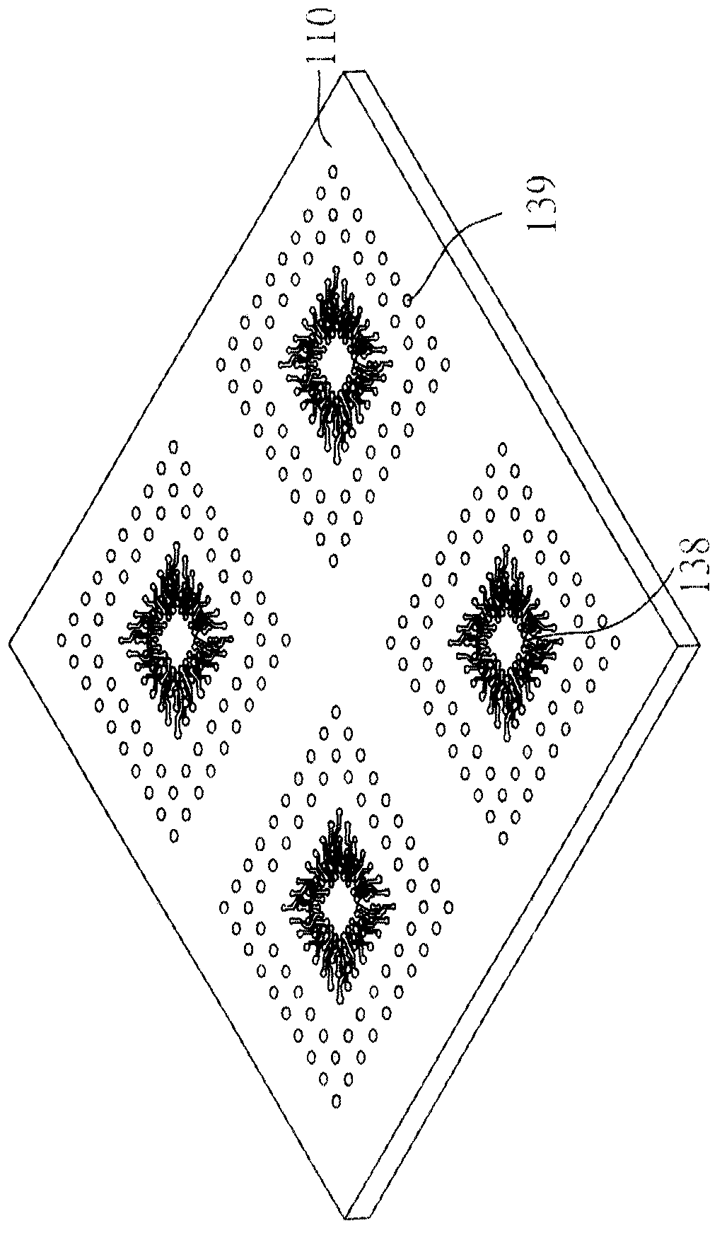
[0056] figure 1 and figure 2 A cross-sectional view and a top perspective view of forming the routing lines 135 on the sacrificial carrier 110 are respectively, wherein the routing lines 135 are formed by metal deposition and metal patterning processes. In this figure, the sacrificial carrier 110 is a single-layer structure, and the routing lines 135 include bonding pads 138 and stacking pads 139 . The sacrificial carrier 110 is typically made of copper, aluminum, iron, nickel, tin, stainless steel, silicon, or other metals or alloys, but any other conductive or non-conductive material may also be used. The thickness of the sacrificial carrier 110 is preferably in the range of 0.1...
Embodiment 2
[0085] Figure 22-Figure 31 In the second embodiment of the present invention, it is a diagram of a method for fabricating a circuit board in which electrical components are embedded in the second reinforcing layer.
[0086] For the purpose of brief description, any descriptions in the above-mentioned Embodiment 1 that can be used for the same application are incorporated herein, and the same descriptions need not be repeated.
[0087] Figure 22 It is a cross-sectional view of the sub-assembly 10 and the first reinforcement layer 20 placed on the carrier film 30 . The subgroup 10 and Figure 10The structures shown are similar, but the only difference is that the sacrificial carrier 110 of this embodiment is a double-layer structure. The sub-assembly 10 is located in the through opening 205 of the first reinforcement layer 20 , and the sacrificial carrier plate 110 is attached to the carrier film 30 . The carrier film 30 is usually an adhesive tape, which can provide tempo...
Embodiment 3
[0103] Figure 34-Figure 37 It is a diagram of a manufacturing method of a circuit board with a third routing circuit in a third embodiment of the present invention.
[0104] For the purpose of brief description, any descriptions in the above embodiments that can be used for the same applications are incorporated herein, and the same descriptions need not be repeated.
[0105] Figure 34 for Figure 29 The cross-sectional view of the third wire 835 formed on the second reinforcing layer 53 of the FIG. The third conductive lines 835 are formed by metal deposition and metal patterning processes, and extend laterally on the outer surface of the second reinforcement layer 53 and contact the vertical connection channels 51 .
[0106] Figure 35 It is a cross-sectional view with a fourth dielectric layer 841 and a fourth blind via 843, wherein the fourth dielectric layer 841 is located on the second reinforcement layer 53 and the fourth conductive line 835, and the fourth blind ...
PUM
 Abstract
Description
Claims
Application Information


