Superconducting circuit structure with step region covered with superconducting cladding layer and preparation method thereof
A technology of area coverage and circuit structure, applied in the manufacture/processing of superconductor devices, superconducting devices, circuits, etc., can solve the problems of Josephson junction stability, poor stability of superconducting circuit structure performance, etc., to improve performance and stability, improve work performance, and avoid damage
- Summary
- Abstract
- Description
- Claims
- Application Information
AI Technical Summary
Problems solved by technology
Method used
Image
Examples
Embodiment 1
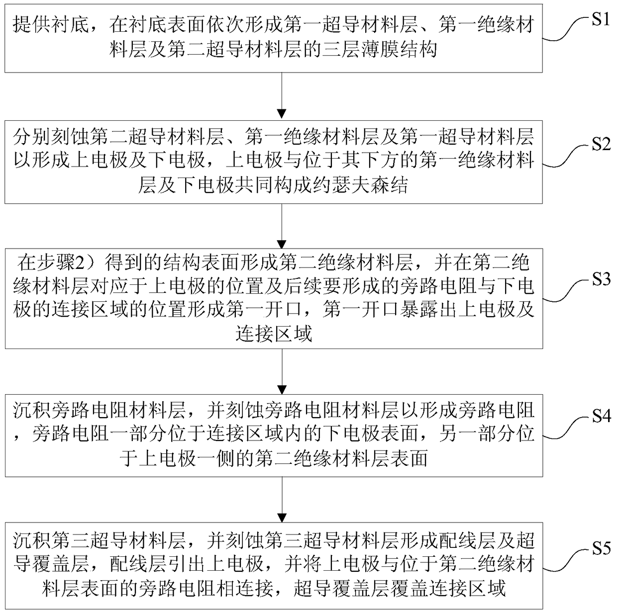
[0066] see image 3 , the present invention provides a method for preparing a superconducting circuit structure with a step region covered with a superconducting coating layer, the method for preparing a superconducting circuit structure with a step region covered with a superconducting coating layer at least includes the following steps:
[0067] 1) providing a substrate, and sequentially forming a three-layer film structure of a first superconducting material layer, a first insulating material layer and a second superconducting material layer on the surface of the substrate;
[0068] 2) Etching the second superconducting material layer, the first insulating material layer and the first superconducting material layer respectively to form an upper electrode and a lower electrode, the upper electrode and the second electrode located below it An insulating material layer and the lower electrode together form a Josephson junction;
[0069] 3) Forming a second insulating material...
Embodiment 2
[0095] read on Figure 11 and Figure 12 , the present invention also provides a superconducting circuit structure with a step region covered with a superconducting covering layer, the superconducting circuit structure having a step region covered with a superconducting covering layer is obtained by the preparation method described in Embodiment 1 or Embodiment 2 Prepared and obtained, the superconducting circuit structure covered with a superconducting covering layer in the step area includes: a substrate 20; a Josephson junction 21, the Josephson junction 21 is located on the surface of the substrate 20, and the Josephson junction 21 From bottom to top, it includes a lower electrode 214, a first insulating material layer 212 and an upper electrode 215; a second insulating material layer 22, and the second insulating material layer 22 covers the substrate 20 and the first insulating material layer 212 surface, the second insulating material layer 22 is provided with a first ...
PUM
| Property | Measurement | Unit |
|---|---|---|
| thickness | aaaaa | aaaaa |
| thickness | aaaaa | aaaaa |
| thickness | aaaaa | aaaaa |
Abstract
Description
Claims
Application Information


