Integrated circuit bypass signal difference amplification sampling system and acquisition method

A bypass signal, integrated circuit technology, applied in program control systems, electrical program control, program control in sequence/logic controllers, etc., can solve the problem that the bypass signal noise interference signal cannot be effectively removed, and the bypass signal is not easy to be accurate. problems such as acquisition, to achieve the effect of improving direct acquisition, improving acquisition accuracy and efficiency, and suppressing logic noise

Inactive Publication Date: 2016-07-06
PEOPLES LIBERATION ARMY ORDNANCE ENG COLLEGE
View PDF11 Cites 2 Cited by
  • Summary
  • Abstract
  • Description
  • Claims
  • Application Information

AI Technical Summary

Problems solved by technology

[0005] The purpose of the present invention is to provide a differential amplification sampling system and acquisition method for integrated circuit bypass signals to solve t...

Method used


Image

  • Integrated circuit bypass signal difference amplification sampling system and acquisition method
  • Integrated circuit bypass signal difference amplification sampling system and acquisition method

Examples


Embodiment 1

[0029] Embodiment 1: An integrated circuit bypass signal differential amplification sampling system.

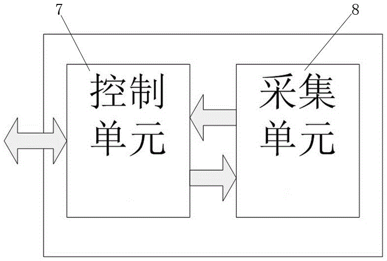
[0030] like figure 1 As shown, the integrated circuit bypass signal differential amplification sampling system of the present invention includes two parts: a control unit 7 and an acquisition unit 8 . The control unit 7 passes through the first data interface 18 ( figure 2 ) is connected with the acquisition unit 8, and is used to control the acquisition process of the acquisition unit 8, send an acquisition interruption signal, adjust delay parameters and filter parameters, receive the acquired digital bypass signal, and pass the second data interface 14 ( figure 2 ) to perform data interaction with the host computer, and send the collected digital bypass signal to the host computer.

[0031]The control unit 7 can be a separate embedded board, such as an FPGA board, or this part of the circuit and the acquisition unit can be integrated on the same board.

[0032] like ...

Embodiment 2

[0037] Embodiment 2: A method for differential amplification and sampling of the bypass signal of the integrated circuit.

[0038] The method for differentially amplifying and sampling integrated circuit bypass signals of the present invention comprises the following steps:

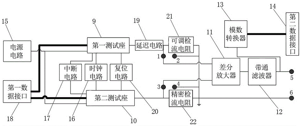
[0039] a. Setting figure 1 and figure 2 A set of IC bypass signal differential amplification sampling system is shown.

[0040] b. Select an integrated circuit chip of the same model and batch as the tested integrated circuit chip, and after chip opening, reverse engineering analysis and logic testing, it can be used as a security chip for comparative testing after being determined to be a security chip; The integrated circuit chip is inserted into the first test socket 9 , and the security chip is inserted into the second test socket 10 .

[0041] c. Lead wires from the first terminal 1 and the second terminal 2 at both ends of the adjustable current-sensing resistor 21 are connected to a channel of ...


PUM


Abstract

The invention relates to an integrated circuit bypass signal difference amplification sampling system and an acquisition method. The sampling system comprises a control unit and a collection unit; the control unit is connected to a collection unit through a first data port for controlling the collection process of the collection unit, transmitting a collection stop signal, regulating delaying parameters and filter parameters, receiving collected a digital bypass signals, and performing data interaction with the upper computer through the second data port; the collection unit comprises a first test socket for inserting the detected integrated circuit chip, a second test socket for inserting the safety chip, a difference amplifier, a band pass filter, an analog-to-digital converter and a second data port; and the first test socket and a second test socket are commonly connected to the same set of the periphery circuit. The integrated circuit bypass signal difference amplification sampling system and acquisition method can obtain the dynamic high accuracy bypass signal of the integrated circuit chip, can effectively inhibit the interference of the logic noise, gets rid of the dependence on the high accuracy oscilloscope, and improves the collection accuracy and collection efficiency on the integrated circuit.

Description

technical field [0001] The invention relates to an integrated circuit detection and processing circuit, in particular to an integrated circuit bypass signal differential amplification sampling system and acquisition method. Background technique [0002] The operation of integrated circuits will cause current fluctuations and electromagnetic radiation, which are called side channel signals (SideChannelSignal, also known as side channel signals) of integrated circuits. The experiment proves that the change of the bypass signal is closely related to the internal structure of the integrated circuit. Once the internal structure of the integrated circuit changes due to aging, defect, interference, tampering and other reasons, the corresponding bypass signal will inevitably change accordingly. Therefore, by using methods such as pattern recognition to analyze changes in the bypass signal, it is possible to detect subtle changes that occur inside the integrated circuit. [0003] T...

Claims


Application Information

Patent Timeline
IPC IPC(8): G05B19/04
CPCG05B19/04G05B2219/26
Inventor 陈开颜李雄伟张阳李艳谢方方韩月霞王骁晗
Owner PEOPLES LIBERATION ARMY ORDNANCE ENG COLLEGE
Why Eureka
Try Eureka