Optimized phase change memory architecture
A phase-change memory and architecture technology, which is applied in the fields of instruments, generation of response errors, electrical digital data processing, etc., can solve problems such as the accumulation of read interference, the inability to fully improve the read voltage, and the different physical characteristics. , to prevent the problem of read interference, increase the length of the check field, and improve the reading speed
- Summary
- Abstract
- Description
- Claims
- Application Information
AI Technical Summary
Problems solved by technology
Method used
Image


Examples
Embodiment 1
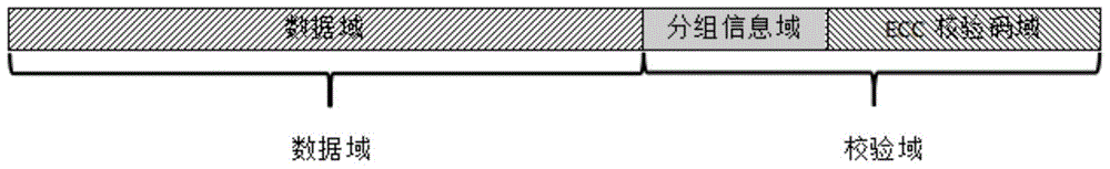
[0048] Assuming that the data field length of a PCM row is 8, the data field grouping process of optimizing the phase-change memory architecture using the present invention comprises the following steps:
[0049] (1) When writing data, when the write voltage rises to the read voltage, the bits that have been written into the data are recorded as vulnerable bits, and the data is written in sequence. During the writing process, according to the position of the vulnerable bits Divide the data domain into four groups. The division process is as follows:
[0050] Because the data length is 8, the 8-bit data field can construct the log 2 8=3 Patterns, the Patterns are:
[0051] Pattern00 (difference characteristic value is 001)
[0052] 1
0
1
0
1
0
1
0
[0053] Pattern01 (difference characteristic value is 010)
[0054] 1
1
0
0
1
1
0
0
[0055] Pattern10 (difference feature value is 100)
...
Embodiment 2
[0066] Assuming that the data field length of a PCM row is 16, the data field grouping flow process of optimizing the phase change memory architecture of the present invention includes the following steps:
[0067] (1) When writing data, when the write voltage rises to the read voltage, the bits that have been written into the data are recorded as vulnerable bits, and the data is written in sequence. During the writing process, according to the position of the vulnerable bits Divide the data domain into four groups. The division process is as follows:
[0068] The 16-bit data field can construct the log 2 16 = 4 Patterns, the index length needs to be log 2 (log 2 16)=2, the Patterns are:
[0069] Pattern00 (difference characteristic value is 0001)
[0070] 1
0
1
0
1
0
1
0
1
0
1
0
1
0
1
0
[0071] Pattern01 (difference characteristic value is 0010)
[0072] 1
1
0
0
1
...
PUM
 Abstract
Description
Claims
Application Information