Printed circuit board (PCB) wiring method and apparatus, and printed circuit board

A technology of printed circuit boards and wiring methods, applied in the directions of printed circuits, printed circuit manufacturing, printed circuit components, etc., can solve the problems of discontinuous impedance and signal integrity of single-ended signal lines and differential signal lines

Inactive Publication Date: 2016-07-06
ZTE CORP
View PDF3 Cites 6 Cited by
  • Summary
  • Abstract
  • Description
  • Claims
  • Application Information

AI Technical Summary

Problems solved by technology

[0003] The present invention provides a printed circuit board wiring method, device and printed circuit board, which solves the problem of discontinuous impedance between single-ended sig

Method used


Image

  • Printed circuit board (PCB) wiring method and apparatus, and printed circuit board
  • Printed circuit board (PCB) wiring method and apparatus, and printed circuit board
  • Printed circuit board (PCB) wiring method and apparatus, and printed circuit board

Examples


Embodiment 2

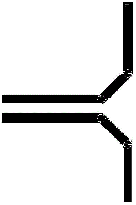
[0072] Figure 4 , 5 The structural diagrams of the single-ended signal line, the differential signal line wiring mode, and the arc-shaped connection signal line wiring mode in the SMA head area provided by Embodiment 2 of the present invention, as shown in Figure 4 , 5 As shown, this embodiment takes the wiring method of the SMA head as an example for illustration. Due to the physical size and twisting restrictions of the SMA head, the outgoing part of the SMA head must use a single-ended signal line to go out, and then the single-ended signal line is converted to a single-ended signal line. Differential signal lines, the wiring method is:

[0073]Make the single-ended impedance of the outgoing single-ended signal line 1 / 2 of the differential impedance of the differential signal line, use software to calculate the line width of the single-ended signal line, the line width and line spacing of the differential signal line, and place the single-ended wiring on the PCB Corres...

Embodiment 3

[0076] Figure 7 The structural schematic diagram of the wiring mode in the BGA area provided by Embodiment 3 of the present invention, as shown in Figure 7 As shown, this embodiment takes the wiring method of the BGA area as an example for illustration. Due to the limitation of the width of the routing channel, the existing method generally uses single-ended signal line routing in the part of the BGApin pin outlet, and in the BGA routing channel area Use smaller line width and line spacing, and use normal wiring outside the BGA area. However, this wiring method makes the line width of the differential signal line in the BGA area smaller, which will increase the loss. At the same time, the reduction of the line width will also increase the difference between the single-ended impedance and the differential impedance at the pin outlet, and Inside and outside the BGA area, the inflection points of different line widths and line spacing conversions will also produce impedance di...

Embodiment 4

[0079] Figure 8 A schematic structural diagram of a printed circuit board wiring device provided in Embodiment 4 of the present invention, as shown in Figure 8 As shown, the PCB wiring device includes:

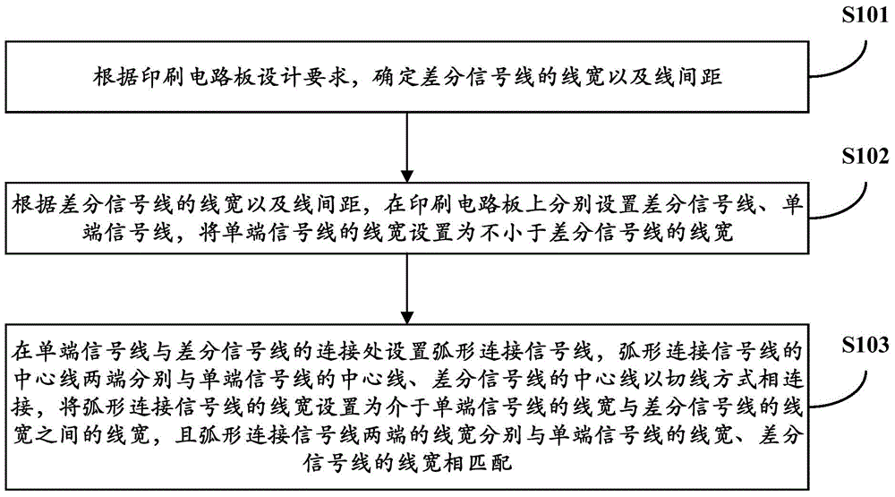
[0080] Determination module 1, used to determine the line width and line spacing of the differential signal lines according to the design requirements of the printed circuit board;

[0081] The wiring module 2 is used to respectively arrange differential signal lines and single-ended signal lines on the printed circuit board according to the line width and line spacing of the differential signal lines determined by the determination module 1, and set the line width of the single-ended signal lines to not less than The line width of the differential signal line; it is also used to set an arc connection signal line at the connection between the single-ended signal line and the differential signal line, and the two ends of the center line of the arc connection signal line are ...


PUM


Abstract

The invention provides a printed circuit board (PCB) wiring method and apparatus, and a PCB. The method comprises the following steps: determining the linewidth and the line spacing of a difference signal line; according to the linewidth and the line spacing of the difference signal line, respectively arranging the difference signal line and a single-end signal line on the PCB, and setting that the linewidth of the single-end signal line is not smaller than the linewidht of the difference signal line; arranging an arc connection signal line at a connecting position between the single-end signal line and the difference signal line, respectively connecting the two ends of a center line of the arc connection signal line with a center line of the single-end signal line and a center line of the difference signal line in a tangent mode, setting that the linewidth of the arc connection signal line is a linewidth ranging from the linewidth of the single-end signal line to the linewidth of the difference signal line, and respectively matching the linewidths of the two ends of the arc connection signal line with the linewidth of the single-end signal line and the linewidth of the difference signal line. Through such a technical scheme, the problem of signal integrity caused by impedance discontinuity between the single-end signal line and the difference signal line is solved.

Description

technical field [0001] The present invention relates to the field of PCB (Printed Circuit Board, printed circuit board) wiring design, in particular to a printed circuit board wiring method, device and printed circuit board. Background technique [0002] In a single board, the high-speed serial wiring generally adopts a differential mode, thereby reducing the interference of external common-mode signals to it and improving the signal-to-noise ratio. However, for areas such as SMA (SmallAType, microwave high-frequency connector) headers, connectors, or BGA (BallGridArray, ball grid array structure) pins, due to the limitation of wiring space or device structure, the part of the pin pin outlet cannot be made differential The structure needs to be converted to differential wiring after going through single-ended wiring. figure 1 , 2 They are the structural diagrams of the existing SMA head and BGA regional wiring methods, such as figure 1 , 2 As shown, the current wiring me...

Claims


Application Information

Patent Timeline
IPC IPC(8): H05K1/02H05K3/00
CPCH05K1/02
Inventor 熊旺马峰超朱顺临
Owner ZTE CORP
Why Eureka
Try Eureka