Polymer light emitting diode structure, manufacturing method, display substrate, and display device

A technology of light-emitting diodes and polymers, applied in the directions of organic semiconductor devices, semiconductor devices, electrical components, etc., can solve the problems of adverse effects on the service life of sub-pixels and lighting quality, non-uniform current flowing through thin films, etc.

Inactive Publication Date: 2016-07-13
BOE TECH GRP CO LTD
View PDF4 Cites 7 Cited by
  • Summary
  • Abstract
  • Description
  • Claims
  • Application Information

AI Technical Summary

Problems solved by technology

In addition, the current flowing through the peripheral part may be higher, causing the current flowing through the film to be non-uniform
Subpixel lifetime and illumination quality may be adversely affected by coffee ring formation

Method used


Image

  • Polymer light emitting diode structure, manufacturing method, display substrate, and display device
  • Polymer light emitting diode structure, manufacturing method, display substrate, and display device

Examples


Embodiment Construction

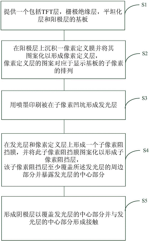
[0031] In order for those skilled in the art to better understand the technical solutions of the present invention, a display panel and a display device provided by the present invention will be further described in detail below with reference to the drawings and specific embodiments. Wherever possible, the same reference numbers will be used throughout the drawings to refer to the same or like parts.

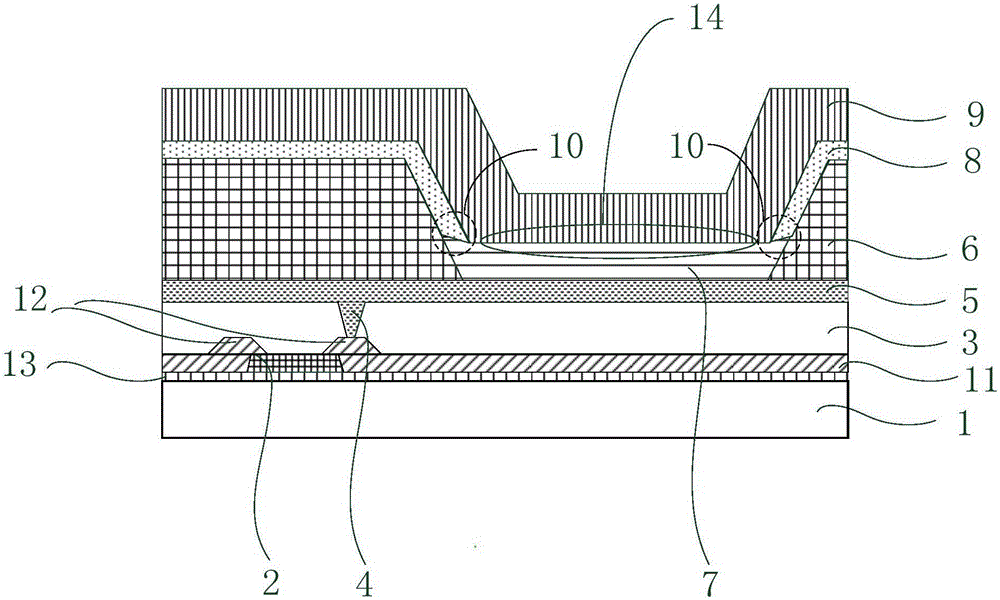
[0032] The invention provides a polymer (PLED) light emitting diode structure.

[0033] figure 1 A cross-sectional view of an exemplary PLED structure is shown. The PLED structure may include a substrate 1, an isolation layer 13, a thin film transistor array (TFT) layer 2, a gate insulating layer 11, a planarization layer 3, a via hole 4, an anode layer 5, a pixel definition layer 6, a light emitting layer 7, A sub-pixel blocking layer 8, and a cathode layer 9. For illustrative purposes, figure 1 Only the source and drain of one TFT of said TFT layer 2 are shown, indicated ...


PUM


Abstract

The invention provides a polymer light emitting diode (PLED) structure. The PLED structure comprises: a substrate, a positive pole layer arranged on the substrate, a pixel defining layer for defining a display area with multiple pixels; a light-emitting layer located in an sub-pixel of each pixel and used for emitting colored light; and a sub-pixel barrier layer arranged between the pixel defining layer and a negative pole layer and used for covering a peripheral part of the light-emitting layer and exposing from a center part of the light-emitting layer. The sub-pixel barrier layer is vertically projected on the substrate and partially coincides with vertical projection of the peripheral part of the light-emitting layer on the substrate. The center part of the light-emitting layer contacts the negative pole layer.

Description

technical field [0001] The present invention relates to display technology, in particular to a polymer light-emitting diode structure, a related display substrate, a display device, and a manufacturing method. Background technique [0002] Ink-jet printed light-emitting devices, such as polymer light-emitting diode (PLED) display products, are easy to produce and have good cost-effectiveness. Applying inkjet printing technology to manufacture PLED display products is easy to implement, and can be used to manufacture large-size display products. With the advancement of high-performance polymers and thin film preparation methods, PLED display products are widely adopted. [0003] In inkjet printing technology, the hole transport layer (hole transport layer, HTL) material, such as poly (3,4-ethylene): poly (4-styrene sulfonate) (PEDOT: PSS), and contains emission Conductive coloring solutions or coloring inks with chemical compositions of different colors such as red, green, ...

Claims


Application Information

Patent Timeline
Patent Type & Authority Applications(China)
IPC IPC(8): H01L33/00H01L33/44H01L33/54
CPCH01L33/005H01L33/44H01L33/54H10K59/122H10K50/82H10K50/865H10K50/11H10K50/81H10K59/124H10K59/1213H10K71/00H10K2102/00H10K2102/351
Inventor 崔颖胡春静
Owner BOE TECH GRP CO LTD
Why Eureka
Try Eureka