AMOLED (active matrix organic light emitting diode) display apparatus

A display device and display unit technology, applied in static indicators, instruments, semiconductor devices, etc., can solve the problems of reduced yield, inability to see GIP circuit 3, abnormal display, etc., to reduce short-circuit conditions, facilitate bad analysis and The effect of testing and improving yield

Active Publication Date: 2016-07-20
KUNSHAN GO VISIONOX OPTO ELECTRONICS CO LTD
View PDF7 Cites 17 Cited by
  • Summary
  • Abstract
  • Description
  • Claims
  • Application Information

AI Technical Summary

Problems solved by technology

[0004] In order to reduce the lap resistance between the cathode 4 and the anode metal 2, the anode metal 2 is generally made wider to cover the entire GIP circuit 3. Since the anode metal 2 is opaque, the GIP circuit 3 cannot be seen through the front. Can view GIP circuit 3 from the back, which brings great inconvenience to poor analysis and signal testing
[0005] At the same time, because the circuit of the GIP circuit 3 is complicated, and the entire surface of the GIP circuit 3 is covered by the cathode 4, if there are impurities, it is easy to cause the conduction of the two, and it is easy to cause various display abnormalities and reduce the yield.

Method used


Image

  • AMOLED (active matrix organic light emitting diode) display apparatus
  • AMOLED (active matrix organic light emitting diode) display apparatus
  • AMOLED (active matrix organic light emitting diode) display apparatus

Examples


Embodiment Construction

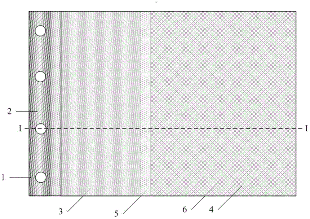
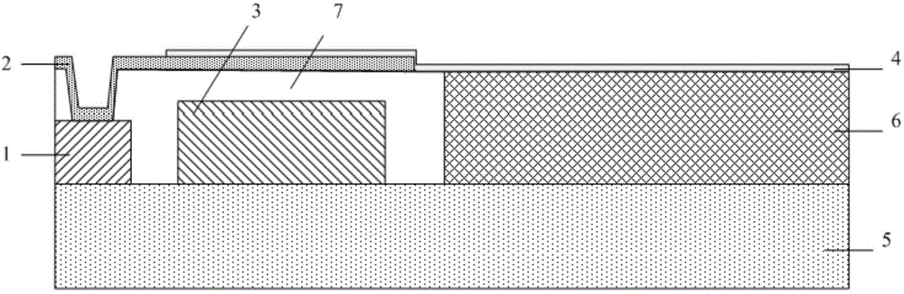
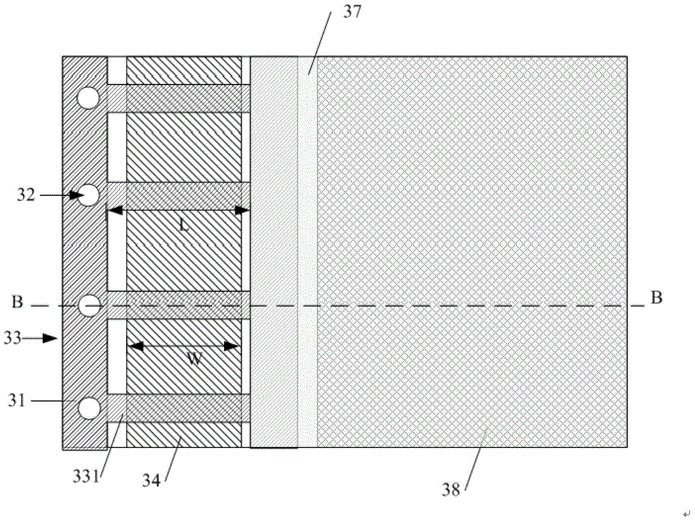
[0022] The AMOLED display device of the present invention will be described in more detail below with reference to schematic diagrams, which represent preferred embodiments of the present invention. It should be understood that those skilled in the art can modify the present invention described here while still achieving the beneficial effects of the present invention. Therefore, the following description should be understood as the broad knowledge of those skilled in the art, but not as a limitation of the present invention.

[0023] In the following paragraphs the invention is described more specifically by way of example with reference to the accompanying drawings. Advantages and features of the present invention will be apparent from the following description and claims. It should be noted that all the drawings are in a very simplified form and use imprecise scales, and are only used to facilitate and clearly assist the purpose of illustrating the embodiments of the presen...


PUM


Abstract

The invention discloses an AMOLED (active matrix organic light emitting diode) display apparatus. The display apparatus comprises a substrate, and a positive electrode, a display unit and a negative electrode which are laminated on the substrate in sequence, wherein a gate in panel (GIP) circuit and a driving voltage negative electrode line are arranged on the periphery of the display unit towards the substrate in sequence; the display apparatus also comprises positive electrode metal; the positive electrode metal crosses over the GIP circuit to be connected with the driving voltage negative electrode line and the negative electrode; the part, overlapped with the projection of the GIP circuit, of the positive electrode metal in a direction perpendicular to the substrate is hollow-out. According to the display apparatus, the positive electrode metal above the GIP circuit is hollow-out, so that the most of the GIP circuit can be exposed, and only a small area of the GIP circuit is covered with the positive electrode metal; therefore, the GIP circuit can be seen clearly from both of the front surface and the back surface, so that disqualification analysis and test can be carried out conveniently; and meanwhile, the condition of short circuit between the negative electrode and the GIP circuit is effectively reduced.

Description

technical field [0001] The invention relates to the field of organic light-emitting display, in particular to an AMOLED display device. Background technique [0002] With the vigorous development of flat panel display technology, active matrix organic light emitting diode (Active Matrix Organic Light Emitting Diode, AMOLED) display devices have been widely used. Compared with the traditional liquid crystal display (Liquid Crystal Display, LCD), in addition to being lighter and thinner, it has excellent characteristics such as self-illumination, low power consumption, no need for backlight, no viewing angle limitation, and high response rate. It has become the current flat-panel display technology. in the mainstream. [0003] figure 1 with figure 2 A common AMOLED display device is shown. Including a substrate 5, an anode (not shown in the figure), a display unit and a cathode 4 sequentially formed on the substrate 5, an on-board gate drive circuit (Gateinpanel, GIP circ...

Claims


Application Information

Patent Timeline
Patent Type & Authority Applications(China)
IPC IPC(8): H01L27/32H01L51/52G09G3/32
Inventor 赵海廷魏朝刚
Owner KUNSHAN GO VISIONOX OPTO ELECTRONICS CO LTD
Why Eureka
Try Eureka