
Liquid crystal panel and active matrix substrate used therefor

A liquid crystal panel and active matrix technology, applied in the field of liquid crystal panels and active matrix substrates, can solve the problem of high pixel aperture ratio and achieve the effect of suppressing flickering

Inactive Publication Date: 2016-07-20
SHARP KK
View PDF10 Cites 3 Cited by
  • Summary
  • Abstract
  • Description
  • Claims
  • Application Information

AI Technical Summary

Problems solved by technology

[0006] For example, in a small, high-definition display device used in a smartphone, etc., it is difficult to increase the aperture ratio of the pixel due to restrictions on the minimum width of wiring (processing conditions) and the like.

Method used


Image

  • Liquid crystal panel and active matrix substrate used therefor
  • Liquid crystal panel and active matrix substrate used therefor
  • Liquid crystal panel and active matrix substrate used therefor

Examples


Embodiment approach 1

[0067] Figure 5 (a) and (b) are a cross-sectional view and a plan view showing a region corresponding to one pixel of the TFT substrate 10A included in the liquid crystal panel of the first embodiment.

[0068] Such as Figure 5 As shown in (a) and (b), the TFT substrate 10A has a gate wiring 2 extending in the horizontal direction provided on the transparent insulating substrate 11, and a gate wiring 2 is provided in a direction (typically a vertical direction) crossing the gate wiring 2. The extended source wiring 4 and the TFT 5 connecting the gate wiring 2 and the source wiring 4 have a structure.

[0069] The TFT 5 includes: a gate electrode 12 connected to the gate wiring 2; a gate insulating layer 20 covering the gate electrode 12; and the source electrode 14 and the drain electrode 15 electrically connected to the oxide semiconductor layer 16 . Source electrode 14 is connected to source wiring 4 . In addition, source electrode 14 and drain electrode 15 are arrange...

Embodiment approach 2

[0080] Figure 6 (a) and (b) are a cross-sectional view and a plan view showing a region corresponding to one pixel of the TFT substrate 10B included in the liquid crystal panel of the second embodiment. In addition, for simplicity of description, the same reference numerals are attached to the same components as those in Embodiment 1, and description thereof will be omitted.

[0081] In the TFT substrate 10B of the present embodiment, pixels are configured such that the feed-through voltage ΔVd1 of the peripheral pixel P1 is smaller than the feed-through voltage ΔVd2 of the central pixel P2 . More specifically, the channel width (the width of the drain electrode 15) of the TFT 5 is designed to be smaller at the peripheral portion of the panel so that Figure 6 In the region C2 surrounded by the dotted line in (b), the parasitic capacitance Cgd between the gate and the drain of the peripheral pixel P1 is smaller than the parasitic capacitance Cgd between the gate and the drai...

Embodiment approach 3

[0086] Figure 7 (a) and (b) are a cross-sectional view and a plan view showing a region corresponding to one pixel of the TFT substrate 10C included in the liquid crystal panel of the third embodiment. In addition, for the sake of simplicity of description, the same reference numerals are assigned to the same components as those in Embodiments 1 and 2, and description thereof will be omitted.

[0087] In the TFT substrate 10C of the present embodiment, pixels are configured such that the feed-through voltage ΔVd1 of the peripheral pixel P1 is smaller than the feed-through voltage ΔVd2 of the central pixel P2 . More specifically, in Figure 7 In a region C3 surrounded by a dotted line in (a), the storage capacitor Cs of the peripheral pixel P1 is set to be larger than the storage capacitor Cs of the central pixel P2.

[0088] In this configuration, the peripheral pixel P1 with a large storage capacitance Cs is less susceptible to the influence of the parasitic capacitance (C...


PUM


Abstract

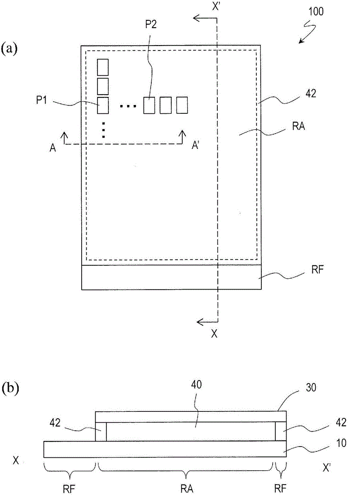
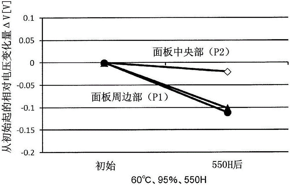
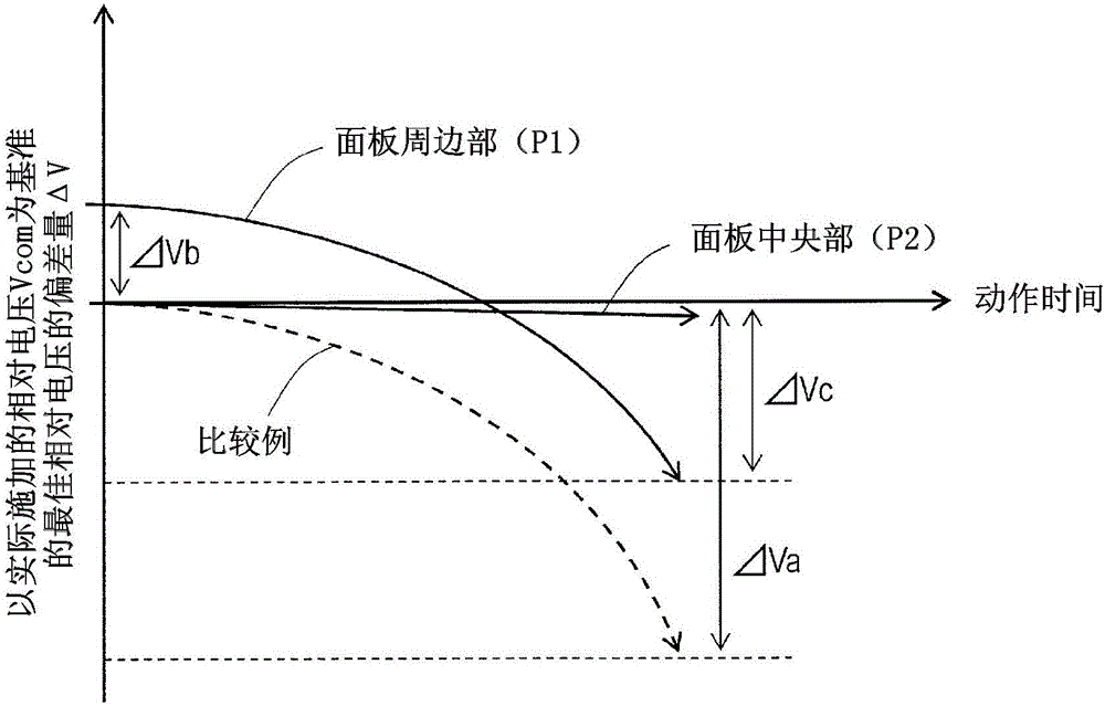
A liquid crystal panel (100) is provided with a pair of substrates (10, 30), a liquid crystal layer (40) retained between the pair of substrates, and a sealing material (42) provided so as to surround the liquid crystal layer. A plurality of pixels (P1, P2) are formed in the shape of a matrix in a region surrounded by the sealing material. Each of the plurality of pixels has an oxide semiconductor TFT (5) provided to one substrate (10) and a pixel electrode (19) that is provided to the one substrate and is connected to the oxide semiconductor TFT. The configuration is such that when the oxide semiconductor TFT is being switched from an on state to an off state, a voltage applied to the liquid crystal layer using the pixel electrode is level-shifted in a negative direction by an amount commensurate with a pull-in voltage Delta Vd. A pull-in voltage Delta Vd1 in the first pixel (P1) among the plurality of pixels is smaller than a pull-in voltage Delta Vd2 in the second pixel (P2) which is positioned farther from the sealing material than the first pixel.

Description

technical field [0001] The present invention relates to a liquid crystal panel and an active matrix substrate having oxide semiconductor TFTs. Background technique [0002] An active matrix substrate used in a liquid crystal display device or the like has a switching element such as a thin film transistor (Thin Film Transistor: hereinafter referred to as “TFT”) for each pixel. As such a switching element, a TFT having an active layer of an amorphous silicon film (hereinafter referred to as "amorphous silicon TFT") or a TFT having a polysilicon film as an active layer (hereinafter referred to as "polysilicon TFT") has been widely used. [0003] In recent years, attempts have been made to use materials other than amorphous silicon and polysilicon as the material of the active layer of the TFT. For example, Patent Document 1 describes a liquid crystal display device in which an active layer of a TFT is formed using an oxide semiconductor film such as InGaZnO (containing oxides...

Claims


Application Information

Patent Timeline
Patent Type & Authority Applications(China)
IPC IPC(8): G02F1/1368G02F1/133G09F9/30G09F9/35G09G3/36
CPCG02F1/136213G02F1/136286G02F1/1368G09G3/3648G09G2320/0219G09G2320/0247G02F1/133388G02F1/1339G02F1/134309G02F2201/123G02F2202/10
Inventor 伊东一笃宫本忠芳内田诚一
Owner SHARP KK
Learn More