LED chip and preparation method thereof

A LED chip, N-type technology, applied in the direction of electrical components, circuits, semiconductor devices, etc., can solve the problems of difficulty in preparing TiW/TiWN structure, difficulty in controlling the stress of TiW single-layer structure, difficulty in TiW/Pt, etc., to ensure light output Efficiency and service life, mature etching process, effect of stress control

Inactive Publication Date: 2016-07-27
LATTICE POWER (JIANGXI) CORP
View PDF3 Cites 2 Cited by
  • Summary
  • Abstract
  • Description
  • Claims
  • Application Information

AI Technical Summary

Problems solved by technology

At present, the mainstream protective layer structures are TiW single-layer structure, TiW / Pt cyclic structure and TiW / TiWN structure. However, these three structures have certain difficulties in the application process. The stress of TiW single-layer structure is difficult to control. It is difficult to perform dry etching, and the preparation of the TiW / TiWN structure is difficult, which is not conducive to the actual control of the production of the protective layer

Method used


Image

  • LED chip and preparation method thereof
  • LED chip and preparation method thereof
  • LED chip and preparation method thereof

Examples


Embodiment 1

[0022] This embodiment adopts the following steps:

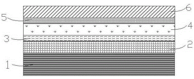
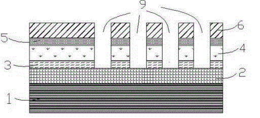
[0023] Such as figure 1 As shown, the MOCVD epitaxial growth technology is used to sequentially grow the N-type GaN layer 2, the active layer 3, and the P-type GaN layer 4 on the sapphire substrate 1; use the evaporation method to deposit Ag on the surface of the P-type GaN layer 4 as Ohmic contact and metal reflective layer 5; on the metal reflective layer 5, a protective metal layer 6 is evaporated, and the structure of the protective metal layer is as follows figure 2 shown; as image 3 As shown, the ICP dry etching method is used to etch a part of the surface of the metal reflective layer until the N-type GaN is exposed to form an N-type electrode hole 9; Figure 4 As shown, SiO was deposited by PECVD 2 passivation layer 10; evaporation of P electrode 11 and N electrode 12; finally, cutting and separating the chip to obtain a single LED chip.

Embodiment 2

[0025] This embodiment adopts the following steps:

[0026] The difference between this embodiment and the LED chip preparation method provided in Embodiment 1 is that Ag is deposited on the surface of the P-type GaN layer 4 as an ohmic contact and the metal reflective layer 5, and then the metal reflective layer 5 is etched, as shown in FIG. Figure 5 As shown, the etching stops until the surface of the P-type GaN layer 4; then a metal protective layer 6 is deposited on the etched Ag layer and the surface of the P-type GaN; as Figure 6 As shown, the etching on the surface of the protective metal layer along the edge of the etching of the reflective metal layer 5 stops at the surface of the N-type GaN, so that the side of the metal reflective layer 5 is covered by the protective metal layer 6 .

Embodiment 3

[0028] This embodiment adopts the following steps:

[0029] The difference between this embodiment and the LED chip preparation method provided in Embodiment 1 is that, after depositing Ag on the surface of the P-type GaN layer 4 as an ohmic contact and the metal reflective layer 5, the metal reflective layer 5 is etched, such as Figure 7 As shown, the etching stops until the surface of the P-type GaN layer 4; then a metal protective layer 6 is deposited on the etched Ag layer and the surface of the P-type GaN; as Figure 8 As shown, the protective metal layer 6 is etched using the ICP etching method, and the etched area is slightly smaller than the etched metal reflective layer Ag, so that the side of the metal reflective layer Ag covers the protective metal layer 6; as Figure 9 As shown, the P-type GaN layer and the active layer are etched again to form N-type electrode holes, and the N-type electrode holes are smaller than the holes etched out of the metal layer 6 .


PUM


Abstract

The present invention discloses an LED chip and a preparation method thereof. The LED chip is characterized in that an N type GaN layer, an active layer, and a P type GaN layer are oderly formed on a substrate, a metal reflective layer is deposited on the surface of the P type GaN layer, a protection metal layer is formed at the surface of the metal reflective layer, the protection metal layer is multi-layer metal Ti and alloy metal TiW layer and is a TiW / Ti structure or TiW / Ti / TiW structure, a partial area of the surface of the protection metal layer is etched with a depth to expose N type GaN, and an N type electrode hole is formed. By using the LED chip prepared by using the technical scheme provided by the invention, the metal reflective layer can be protected well, the light emitting efficiency and service life can be ensured, the stress is controlled well, the cost is low, the etching process is mature, and the operation is convenient.

Description

technical field [0001] The invention relates to the field of semiconductor light emitting diodes, in particular to an LED chip and a preparation method thereof. Background technique [0002] The LED chip emits light by applying a forward current to the PN junction, and the free electrons and holes recombine to emit light. However, the emitted light scatters to the surroundings, which affects the light extraction efficiency of the chip. A layer of metal layer with high reflectivity is made, so that the light emitted by the quantum well is reflected by the metal layer with high reflectivity, the direction of light is controlled, and the light extraction efficiency is improved. However, it is vulnerable to damage, which affects the reflection efficiency of the metal layer and the quality of the chip. For example, the current mainstream metal reflection layer material is silver. In a humid environment with a DC voltage gradient, water molecules penetrate into the surface of the ...

Claims


Application Information

Patent Timeline
IPC IPC(8): H01L33/10H01L33/48
Inventor 彭翔
Owner LATTICE POWER (JIANGXI) CORP
Why Eureka
Try Eureka