Display device with NFC function

A display device and functional technology, applied in the direction of antenna support/installation device, input/output process of data processing, instrument, etc., can solve the problems of increasing frame size, easy dislocation, easy wear, etc., and achieve high reliability, The effect of shortening the communication distance and good market prospects

Active Publication Date: 2016-08-03
SUZHOU QUINGYUE OPTOELECTRONICS TECH CO LTD
View PDF5 Cites 18 Cited by
  • Summary
  • Abstract
  • Description
  • Claims
  • Application Information

AI Technical Summary

Problems solved by technology

However, in order to ensure the wiring space of the NFC antenna in such a solution, the NFC wire frame must be made very large, thereby increasing the frame size of the entire module outside the display area
This solution solves the problem of easy wear and misalignment of conventional NFC antenna wiring to a certain extent, but the excessively large module frame size is also not conducive to the design of small electronic devices

Method used


Image

  • Display device with NFC function
  • Display device with NFC function
  • Display device with NFC function

Examples


no. 1 example

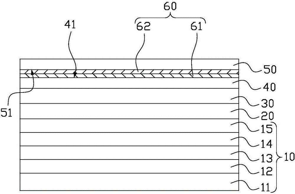
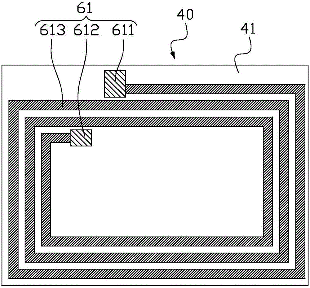
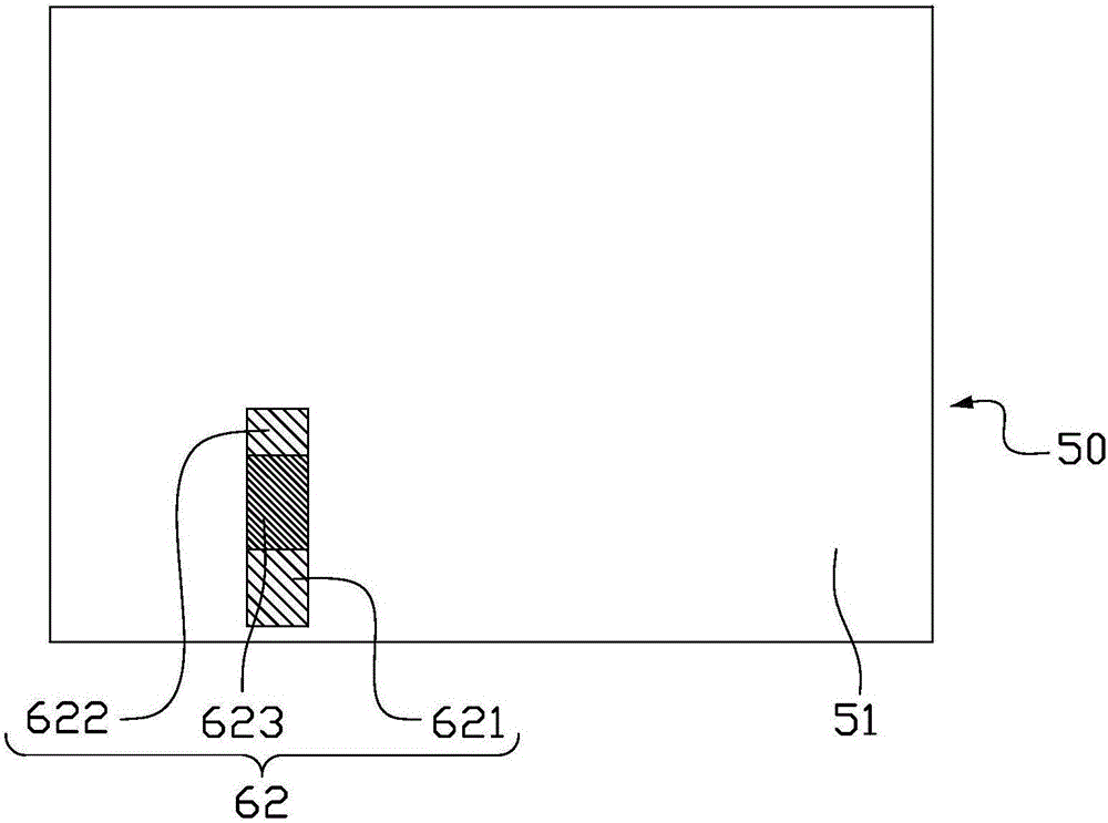
[0047] figure 1 It is a schematic structural diagram of the display device in the first embodiment of the present invention, please refer to figure 1 , the display device includes a display panel 10 , a shielding layer 20 , a touch sensing layer 30 , a first transparent film 40 and a second transparent film 50 . In this embodiment, the display panel 10, the shielding layer 20, the touch-sensitive layer 30, the first transparent film 40, and the second transparent film 50 are sequentially stacked, that is, the shielding layer 20 is arranged on the display panel 10, and the touch-sensitive layer 30 is arranged on the display panel 10. On the shielding layer 20 , the first transparent film 40 is disposed on the touch-sensitive layer 30 , the second transparent film 50 is disposed on the first transparent film 40 , and the various structural layers can be pasted by transparent optical adhesive (OCA). In other embodiments, the positions of the first transparent film 40 and the sec...

no. 2 example

[0056] Figure 4 It is a schematic structural diagram of the display device in the second embodiment of the present invention, please refer to Figure 4 , the display device includes a display panel 10, a shielding layer 20, a touch sensing layer 30 and a transparent film 40a. In this embodiment, the display panel 10, the shielding layer 20, the touch-sensitive layer 30 and the transparent film 40a are sequentially stacked, that is, the shielding layer 20 is arranged on the display panel 10, the touch-sensitive layer 30 is arranged on the shielding layer 20, and the transparent film 40 a is disposed on the touch sensing layer 30 , and the various structural layers can be bonded by transparent optical adhesive (OCA).

[0057] The display panel 10 is, for example, an OLED display panel, an electronic paper (E-ink) display panel, an LCD display panel, and the like. In this embodiment, the display panel 10 is an OLED display panel and includes an OLED panel encapsulation cover 1...

no. 3 example

[0064] Figure 7 It is a schematic structural diagram of the display device in the third embodiment of the present invention, please refer to Figure 7 , the display device includes a display panel 10, a shielding layer 20, a touch sensing layer 30 and a transparent film 40b. In this embodiment, the display panel 10, the shielding layer 20, the touch-sensitive layer 30 and the transparent film 40b are sequentially stacked, that is, the shielding layer 20 is arranged on the display panel 10, the touch-sensitive layer 30 is arranged on the shielding layer 20, and the transparent film 40b is disposed on the touch sensing layer 30, and the various structural layers can be pasted together by transparent optical adhesive (OCA).

[0065] The display panel 10 is, for example, an OLED display panel, an electronic paper (E-ink) display panel, an LCD display panel, and the like. In this embodiment, the display panel 10 is an OLED display panel and includes an OLED panel encapsulation c...


PUM


Abstract

The invention discloses a display device with an NFC function. The display device comprises a display panel, wherein NFC antenna routing is integrally arranged in the display device; the NFC antenna routing is positioned on one side, with a display surface, of the display panel, and is made from transparent conductor materials. According to the display device disclosed by the invention, the NFC antenna routing is integrally arranged in the display device, made from the transparent conductor materials and positioned on the display surface close to the display panel, so that the sensitivity of an NFC signal is high and the reliability of the NFC signal is high; the NFC antenna routing is not liable to damage and deviate; the NFC antenna routing is made from the transparent conductor materials, so that the NFC antenna routing can be placed in a display area, and the design of a narrow frame of a die set is facilitated.

Description

technical field [0001] The invention relates to the field of display technology, in particular to a display device with NFC function. Background technique [0002] There are many types of display technologies, including liquid crystal display (Liquid Crystal Display, LCD) and organic light-emitting diode display (organic light-emitting diode, OLED). Among them, OLED display is very attractive, which has the advantages of self-luminous display, thin and light power saving, etc. It can also be made of flexible display based on flexible materials, which can be rolled, folded or used as a part of wearable devices. The light-emitting principle of OLED is to deposit a very thin organic light-emitting material between two electrodes, pass a current to the organic light-emitting material, and cause light emission through carrier injection and recombination. [0003] Graphene is the thinnest and hardest nano-material known in the world, it is almost completely transparent, absorbing...

Claims


Application Information

Patent Timeline
Patent Type & Authority Applications(China)
IPC IPC(8): G06F1/16G06F3/041H01L27/32H01Q1/22
CPCH01Q1/22G06F1/1601G06F3/041H10K59/10
Inventor 穆欣炬李鹏云鲁凤娟
Owner SUZHOU QUINGYUE OPTOELECTRONICS TECH CO LTD
Why Eureka
Try Eureka