Formation method of flash

A flash memory and flat-layer technology, which is applied in the fields of electrical components, semiconductor/solid-state device manufacturing, circuits, etc., can solve the problems of flash memory data retention (data retention) decline and other issues

Active Publication Date: 2016-08-03
SEMICON MFG INT (SHANGHAI) CORP
View PDF6 Cites 6 Cited by
  • Summary
  • Abstract
  • Description
  • Claims
  • Application Information

AI Technical Summary

Problems solved by technology

[0004] However, the formation method of the existing flash memory leads to the phenomenon that the data retention (data retention) capability of the formed flash memory is prone to decrease.

Method used


Image

  • Formation method of flash
  • Formation method of flash
  • Formation method of flash

Examples


Embodiment Construction

[0029] As mentioned in the background, the existing methods for forming flash memory lead to the phenomenon that the formed flash memory is prone to decline in data retention capability, that is, data loss is prone to occur.

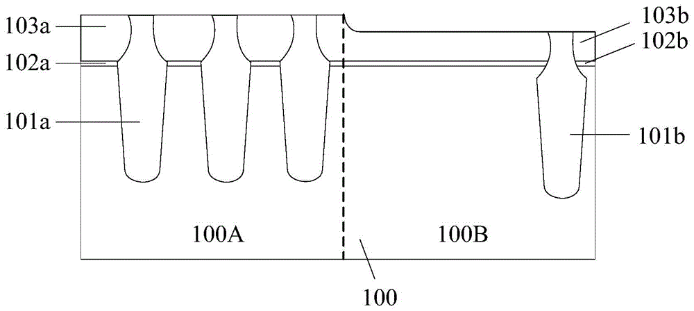
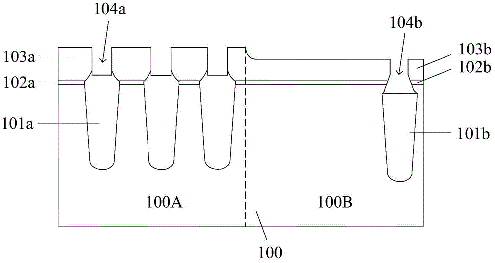
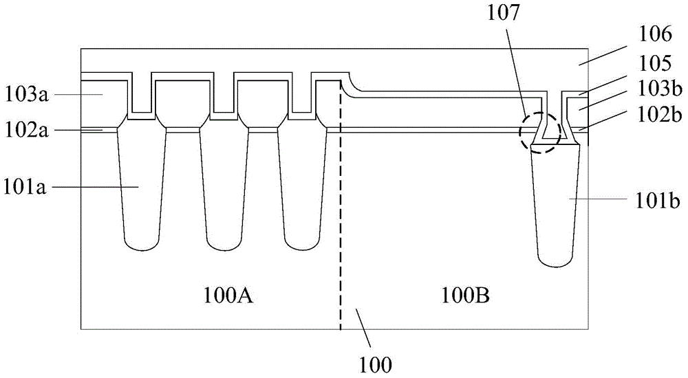
[0030] Figure 1 to Figure 3 A schematic structural diagram corresponding to each step of the existing flash memory forming method is shown.

[0031] Please refer to figure 1 , a semiconductor substrate 100 is provided, and the semiconductor substrate 100 includes a core region 100A and a peripheral region 100B. And a tunneling dielectric layer is formed on the semiconductor substrate 100, and the tunneling dielectric layer located on the core region 100A is the tunneling dielectric layer 102a. The tunneling dielectric layer on the peripheral region 100B is the tunneling dielectric layer 102b. The core area 100A and the peripheral area 100B are separated by a dotted line (not marked) to show the difference.

[0032] Please continue to refer figure ...


PUM


Abstract

The invention relates to a formation method of a flash. The formation method comprises the steps of providing a semiconductor substrate, wherein the semiconductor substrate comprises a core region and a peripheral region, forming shallow trench isolation structures with the top being higher than the semiconductor substrate in the core region and the peripheral region, forming a tunneling dielectric layer on the semiconductor substrate, forming a floating gate on the tunneling dielectric layer, wherein the thickness of the floating gate in the core region is greater than the thickness of the floating gate in the peripheral region, forming a leveling layer on the shallow trench isolation structures and the floating gate, wherein the upper surface of the leveling layer on the core region is flush with the upper surface of the leveling layer on the peripheral region, removing the leveling layer and the top of the shallow trench isolation structures so as to form grooves and exposing the top and the side surface of the floating gate again, forming a gate dielectric layer at the upper surface and the side surface of the floating gate, and forming a control gate on the gate dielectric layer. The formation method provided by the invention improves the data reservation capacity of the formed flash and improves the reliability of the flash.

Description

technical field [0001] The invention relates to the field of semiconductor manufacturing, in particular to a method for forming a flash memory. Background technique [0002] Flash memory (Flash), also known as flash memory, has become the mainstream of non-volatile memory. According to different structures, flash memory can be divided into two types: NOR Flash and NAND Flash. Or non-flash memory is suitable for applications such as mobile phones or motherboards that need to record system codes because of its fast reading speed. And non-flash memory is especially suitable for multimedia data storage because of its high density and high writing speed. [0003] Another classification method of flash memory can be divided into two types: floating gate flash memory (floating gate flash) and charge-trapping flash memory (CTF, charge-trapping flash). For flash memory with a floating gate structure, due to the existence of the floating gate, the flash memory can complete the read...

Claims


Application Information

Patent Timeline
Patent Type & Authority Applications(China)
IPC IPC(8): H01L21/8247H01L21/28
Inventor 陈建奇
Owner SEMICON MFG INT (SHANGHAI) CORP
Why Eureka
Try Eureka