Device manufacturing method suitable for low-heat-conduction and electric-conduction material substrate

A technology of conductive materials and low thermal conductivity, which is applied in the field of device manufacturing of low thermal conductivity and conductive material substrates, can solve problems such as pollution, low production capacity, and poor graphics quality, and achieve the effects of simple process flow, high processing precision, and high yield rate

Active Publication Date: 2019-05-21
HANGZHOU LION MICROELECTRONICS CO LTD
View PDF5 Cites 1 Cited by
  • Summary
  • Abstract
  • Description
  • Claims
  • Application Information

AI Technical Summary

Problems solved by technology

This type of production process is relatively simple, but there are still shortcomings and limitations brought about by the properties of the diffractive material itself
[0006] 3) Directly use laser beam or electron beam to write DOE pattern on the mask material layer. This kind of processing has high precision, but it takes a long time and the production capacity is very low.
This patent is aimed at etching heat and electricity poor conductor materials, such as glass. During the reactive plasma dry etching process, the temperature of the substrate increases rapidly due to chemical reactions and ion collisions, and static charges are easily accumulated in local areas, which affects the plasma etching process. The various adverse consequences caused by:
[0009] 1) The photoresist used as an etching mask is denatured and scorched at high temperature and cannot be successfully removed after the etching is completed, or it cannot be used as a mask because the etching rate is too fast at the beginning
[0010] 2) Insulating substrates with poor thermal conductivity have poor etch rate stability and uniformity
Although the method provided by the invention can ensure the stability and uniformity of the etching rate, the disadvantage is that the etching result is very dependent on the control of the coating process of the thermally conductive adhesive, and the thickness and thickness uniformity of the thermally conductive adhesive directly affect the etching process. The final result, batch repeatability, yield, etc.
[0011] In addition, the patent does not involve the etching of different complex patterns, including regular and random patterns, and the etching effects of different patterns with different aspect ratios.
In addition, currently reported dry etching with quartz glass as the substrate material either: 1) It is necessary to use metal as an etching mask to achieve the desired etching selectivity. This process is limited by the metal mask For example, the formation and control of the critical dimensions of metal mask patterns need to be etched by shadow or photolithography, and compared with the traditional photoresist pattern critical dimensions and pattern formation, the pattern quality is poor Many, can not meet the requirements of small-scale device etching, the metal mask needs to be removed later, and the metal mask participating in the etching process will cause pollution caused by secondary deposition on the etching surface and side walls during the etching process; 2) It is difficult to meet the requirements of uniform etching depth and highly vertical etching sidewall morphology for design patterns with different sizes of etching areas at the same time.

Method used


Image

  • Device manufacturing method suitable for low-heat-conduction and electric-conduction material substrate

Examples


Embodiment 1

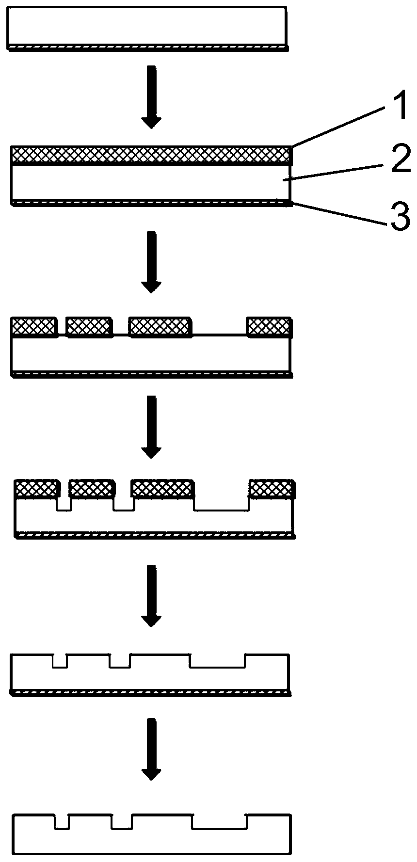
[0056] A device manufacturing method suitable for quartz glass substrates, the process is as follows figure 1 shown, including the following steps:

[0057] 1) A 1000 angstrom thick, opaque conductive film 1 (TiW) is plated on the back of the quartz glass substrate 2 by magnetron sputtering.

[0058] 2) Coating photoresist 3 on the front side of the quartz glass substrate.

[0059] 3) Exposure and development.

[0060] 4) The quartz glass substrate is dry-etched with an inductively coupled plasma dry etching equipment equipped with a unipolar electrostatic adsorption chuck to realize the replication of the graphics on the front side of the quartz glass substrate, and repeat steps 2) and 3) to achieve multi-layer graphics Replication, and complete the replication of various patterns from simple to complex, from uniform depth to multi-layer depth on the quartz glass substrate; The inert gas helium for heat dissipation.

[0061] Wherein, in step 4), the etching gas and auxili...

Embodiment 2

[0066] A method for manufacturing a device suitable for a quartz glass substrate, comprising the following steps:

[0067] 1) A 300 angstrom thick, opaque conductive TiW film was coated on the back of the quartz glass substrate by magnetron sputtering.

[0068] 2) Coating photoresist on the front side of the quartz glass substrate.

[0069] 3) Exposure and development.

[0070] 4) The quartz glass substrate is dry-etched with an inductively coupled plasma dry etching equipment equipped with a mechanical chuck to realize the replication of graphics on the front side of the quartz glass substrate, and repeat steps 2) and 3) to achieve multi-layer graphics replication, And complete the replication of various patterns on the quartz glass substrate from simple to complex, from uniform depth to multi-layer depth; Gas helium for heat dissipation.

[0071] Wherein, in step 4), the etching gas and auxiliary etching gas are selected from the following combination: CF 4 / C 4 f 8 / H...

Embodiment 3

[0076] A method for manufacturing a device suitable for a quartz glass substrate, comprising the following steps:

[0077] 1) A 500 angstrom thick, opaque conductive Cr film is plated on the back of the quartz glass substrate by evaporation process.

[0078] 2) Coating photoresist on the front side of the quartz glass substrate.

[0079] 3) Exposure and development.

[0080] 4) The quartz glass substrate is dry-etched with an inductively coupled plasma dry etching equipment equipped with a bipolar Johnsen-Rahbek type electrostatic adsorption chuck to realize the replication of the pattern on the front side of the quartz glass substrate, and repeat steps 2) and 3) To achieve multi-layer graphics replication, and complete the replication of various graphics on the quartz glass substrate from simple to complex, from uniform depth to multi-layer depth; during the etching process, it needs to be kept on the back of the chuck and the quartz glass Helium, an inert gas with small mo...


PUM

PropertyMeasurementUnit
thicknessaaaaaaaaaa

Abstract

The invention relates to the field of material processing, and discloses a device manufacturing method suitable for a low-heat-conduction and electric-conduction material substrate, which comprises the following steps: 1) plating an electric-conduction film on the back surface of the low-heat-conduction and electric-conduction material substrate; 2) coating photoresist on the front surface of thelow-heat-conduction and electric-conduction material substrate; 3) exposing and developing; 4) loading the low-heat-conduction and electric-conduction material substrate into a substrate tray, carrying out dry etching through inductively coupled plasma dry etching equipment, repeating the step 2) and the step 3) to realize multi-layer graph copying, and completing copying of various graphs from simple to complex and from uniform depth to multi-layer unequal depth; wherein the etching gas is selected from CF4, CHF3, CF4/CHF3, C4F8/CF4 or C4F8/CHF3; the auxiliary etching gas is selected from O2,H2, Ar or N2; 5) stripping the photoresist; and 6) removing a golden electric film. The method has the advantages that the technological process is simple, the processing precision is high, no defectexists, the yield is high, and the mass production can be rapidly realized.

Description

technical field [0001] The invention relates to the field of quartz glass processing, in particular to a device manufacturing method suitable for substrates made of low thermal and electrical conductive materials. Background technique [0002] The 3D sensing and imaging technology triggered by the face recognition function of the iPhone X smartphone will become the fastest-growing emerging high-tech technology industry in the next few years, and the application of 3D imaging and sensing technology is by no means limited to face recognition. The visualization and better-quality imaging based on this technology will continue to rapidly penetrate into computer vision, artificial intelligence, telemedicine, safe navigation, and other applications ranging from ordinary people's home life to commercial, national defense technology, and space exploration. among. Core components such as ToF sensors, vertical cavity surface emitting lasers (VCSEL), diffractive optical elements (DOE)...

Claims


Application Information

Patent Timeline
Patent Type & Authority Applications(China)
IPC IPC(8): G02B5/18
Inventor 任华汪文宇
Owner HANGZHOU LION MICROELECTRONICS CO LTD
Why Eureka
Try Eureka