
CSP packaging structure of power device and manufacturing method thereof

A packaging structure and power device technology, which is applied in semiconductor/solid-state device manufacturing, semiconductor devices, electric solid-state devices, etc., can solve the problems of increasing the on-resistance of power devices and reducing the chip utilization area, and achieve the effect of reducing on-resistance

Active Publication Date: 2019-08-13
SHANGHAI FINE CHIP SEMICON
View PDF4 Cites 0 Cited by
  • Summary
  • Abstract
  • Description
  • Claims
  • Application Information

AI Technical Summary

Problems solved by technology

[0006] One of the technical problems to be solved by the present invention is: in view of the existing CSP packaging method of power devices that reduces the utilization area of ​​the chip and increases the on-resistance of the power device, a method that makes full use of the surface area of ​​the chip and maximizes the possible CSP package structure of power devices to minimize the on-resistance of power devices

Method used


Image

  • CSP packaging structure of power device and manufacturing method thereof
  • CSP packaging structure of power device and manufacturing method thereof
  • CSP packaging structure of power device and manufacturing method thereof

Examples


Embodiment Construction

[0030] In order to make the technical means, creative features, objectives and effects achieved by the present invention easy to understand, the present invention will be further described below in conjunction with specific illustrations.

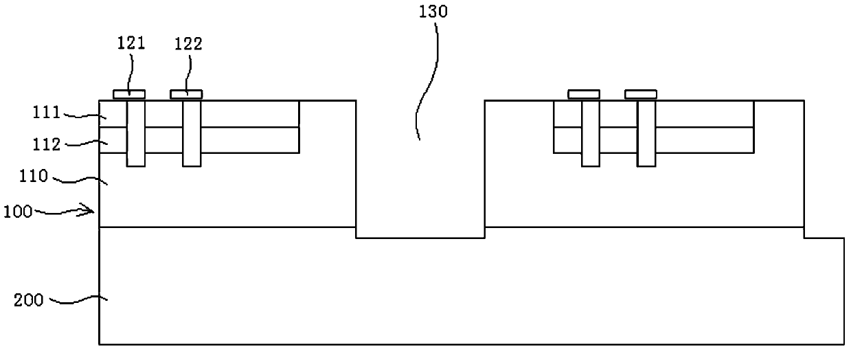
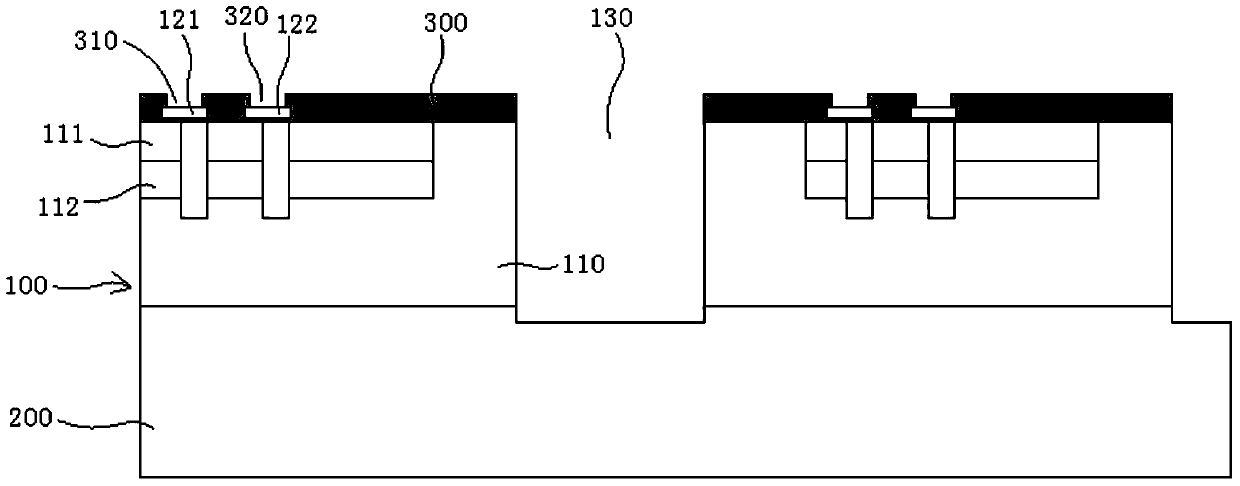
[0031] see Figure 7 , shown in the figure is the CSP packaging structure of the power device, including the chip 100 and the N+ substrate 200 as the drain of the power device arranged on the back of the chip 100, and a number of evenly distributed dies 110 are formed on the front of the chip 100 , each die 110 is provided with an N+ source layer 111 and a P-body layer 112 from top to bottom, and a front surface of each die 110 is provided with an N+ source layer 111 or a P-body layer 112 connected A source bump 121 and a gate bump 122 connected to polysilicon.

[0032] The chip 100 is located between the scribe lane 130 between two adjacent dies 110 and / or the area of ​​the four corners of each die 110 is etched and etched or scribed to t...


PUM


Abstract

A CSP structure of a power device disclosed by the present invention is characterized in that by utilizing the scribing ways between the chips and / or the areas at the four corners of a chip and by using a corrosion or scribing method, the epitaxial layers at the areas are removed to expose an N+ substrate, and then a layer of metal is evaporated and plated on the surface of the chip by a sputtering or evaporation method to lead an N+ layer to the surface, thereby realizing the CSP requirements. The beneficial effects of the present invention are that the surface area of the chip is utilized effectively and fully, and the on-resistance of the power device is reduced greatest possibly.

Description

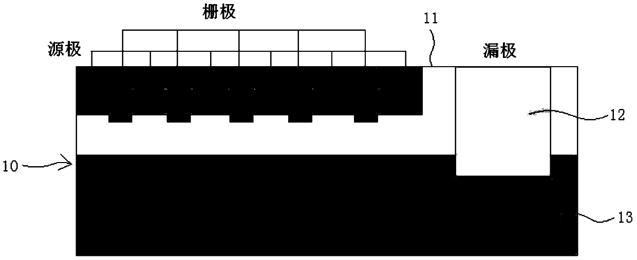
technical field [0001] The invention relates to the technical field of power device preparation, in particular to a CSP package structure of a power device and a manufacturing method thereof. Background technique [0002] CSP technology is a new type of integrated circuit packaging technology developed in recent years. Products packaged with CSP technology have high package sealing, good performance, small size, light weight, and are compatible with surface mount technology, so its development speed is quite fast, and it has become one of the important packaging technologies for integrated circuits. [0003] A power transistor has three electrodes, source / emitter, gate / base and drain / collector. Usually, in order to reduce the on-resistance and make full use of the area of ​​the chip, the source / emitter and gate / base are on the front side of the chip, and the drain / collector are on the back side of the chip. To use CPS technology for packaging, it is necessary to guide the ...

Claims


Application Information

Patent Timeline
Patent Type & Authority Patents(China)
IPC IPC(8): H01L23/488H01L23/485H01L21/60
CPCH01L24/10H01L24/26H01L24/81H01L24/83
Inventor 黄平鲍利华张迪雄
Owner SHANGHAI FINE CHIP SEMICON
Learn More