Planar flying probe tester and PCB transmission method

A flying probe testing machine and PCB board technology, applied in the field of testing machines, can solve the problems of low re-testing efficiency and occupying much time, so as to improve the re-testing efficiency, high test stability and accuracy, reduce the scrap rate and re-testing cost effect

Active Publication Date: 2016-08-10
HANS CNC SCI & TECH
View PDF5 Cites 24 Cited by
  • Summary
  • Abstract
  • Description
  • Claims
  • Application Information

AI Technical Summary

Problems solved by technology

However, the flying probe tester can only be used in small batch production
However, when the circuit board is relatively dense, the failure rate of the general-purpose or special-purpose needle bed machine

Method used


Image

  • Planar flying probe tester and PCB transmission method
  • Planar flying probe tester and PCB transmission method
  • Planar flying probe tester and PCB transmission method

Examples


Embodiment Construction

[0028] Now in conjunction with the accompanying drawings, the preferred embodiments of the present invention will be described in detail.

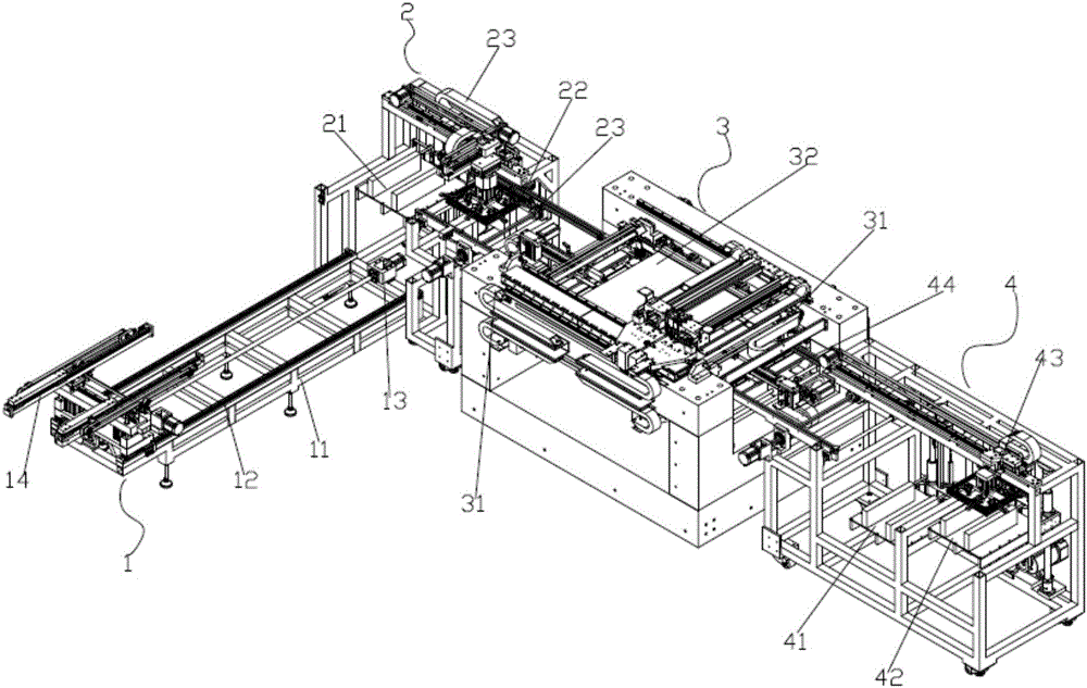
[0029] like figure 1 As shown, the embodiment of the present invention provides a planar flying probe testing machine, including a material receiving mechanism 1 , a material loading mechanism 2 , a flying probe test host 3 and a material unloading mechanism 4 .

[0030] Described material receiving mechanism 1 comprises base 11, and this base 11 is provided with sliding guide rail 12, material fetching driving device 13, and the material fetching mechanism 14 that takes out the unqualified PCB board to be tested of needle bed test table in order, The pick-up device 14 is arranged on the sliding guide rail 12, and the pick-up device 14 is driven to move by the pick-up driving device 13. When the pick-up device 1 receives the pick-up instruction, the pick-up mechanism 14 stretches into the needle bed, and will be placed on the needle bed. ...


PUM


Abstract

The invention provides a planar flying probe tester and a PCB transmission method. The planar flying probe tester includes a material receiving mechanism, consisting of a material take-out mechanism for taking qualified and unqualified PCBs under test out of a probe bed testing material table; a loading mechanism, consisting of a feeding table, a feeding mechanical arm and a feeding conveying device; a flying probe testing host, consisting of a test host conveying device and a test device; and a laying-off mechanism, consisting of a PASS material table, an NG material table, a laying-off mechanical arm and a laying-off motion device. The material receiving mechanism and a probe bed are connected in a seamless manner, the feeding mechanism conveys the PCBs under test to the flying probe testing host and tests the electrical properties thereof, then the laying-off mechanism places the qualified or unqualified PCBs onto the PASS material table or the NG material table, and the test is completed. The test stability and accuracy are high, the retest efficiency is greatly improved, and the scrap rate of the PCBs and the retest cost are also reduced.

Description

technical field [0001] The invention relates to the field of testing machines, in particular to a planar flying probe testing machine and a method for transmitting a PCB board. Background technique [0002] At present, with the rapid development of PCB technology, the development of circuit boards in the direction of light, thin and short is accelerating. Artificial electrical test. When the Pad size of the test board is below 2mil and the density of the Pad pitch is 6mil, coupled with the eccentric holes in the process, the general or professional needle bed cannot meet the test requirements. Only the flying probe test can be overcome by changing the test point in the system. Test the limits of distance. However, the flying probe testing machine can only be used in small batch production. However, when the circuit board is relatively dense, the failure rate of the general-purpose or special-purpose needle bed machine will increase. If the general-purpose or special needl...

Claims


Application Information

Patent Timeline
IPC IPC(8): G01R31/28
CPCG01R31/2806G01R31/2808
Inventor 谭艳萍王星翟学涛杨朝辉高云峰
Owner HANS CNC SCI & TECH
Why Eureka
Try Eureka