FinFET device and manufacturing method thereof, and electronic apparatus
A technology of electronic devices and manufacturing methods, applied in semiconductor/solid-state device manufacturing, semiconductor devices, circuits, etc., can solve the problems of dose loss, failure to control source/drain punch-through, etc., and achieve the effect of enhancing the suppression ability
Inactive Publication Date: 2016-08-10
SEMICON MFG INT (SHANGHAI) CORP
View PDF7 Cites 5 Cited by
- Summary
- Abstract
- Description
- Claims
- Application Information
AI Technical Summary
Problems solved by technology
If the implanted ions for channel stop implantation are boron ions or boron fluorine ions, boron ions or boron fluoride ions are easy to diffuse to the isolation structure during the
Method used
View moreImage
Smart ImageViewing Examples

Examples
 PUM
 Abstract
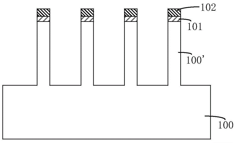
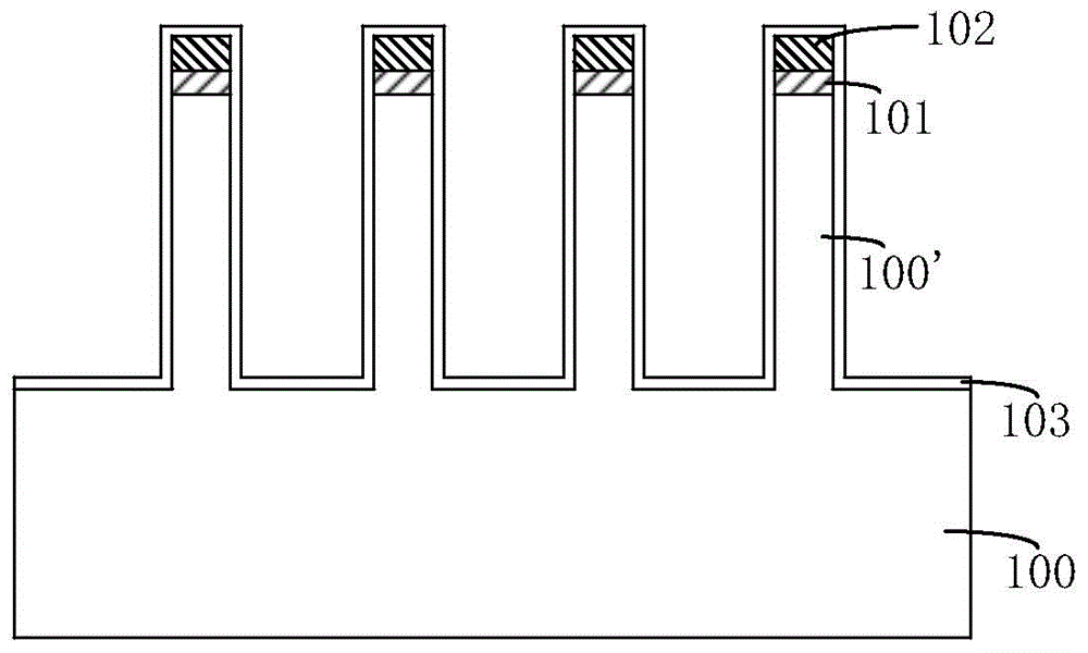
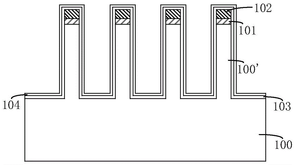
The present invention provides a FinFET device, a manufacturing method thereof, and an electronic device. The method includes: providing a semiconductor substrate, on which a plurality of fins are formed, and a hard mask layer is formed on the top of the fins; forming A layer of liner oxide to cover the surface of the semiconductor substrate, the sidewalls of the fins, and the sidewalls and top of the hard mask layer; a layer of isolation material is deposited to completely fill the gaps between the fins; portions of the fins are exposed , and then form fins with a specific height; sequentially implement well region implantation and channel stop implantation to adjust threshold voltage and control source/drain punchthrough. According to the present invention, by implementing channel stop implantation in which the implanted ions are carbon ions, nitrogen ions or a combination of the two, the source/drain punchthrough suppression capability of the FinFET can be effectively enhanced.
Description
technical field [0001] The invention relates to a semiconductor manufacturing process, in particular to a FinFET device, a manufacturing method thereof, and an electronic device. Background technique [0002] With the continuous development of semiconductor technology, the improvement of integrated circuit performance is mainly achieved by continuously shrinking the size of integrated circuit devices to increase its speed. Currently, as the semiconductor industry has advanced to nanotechnology process nodes in pursuit of high device density, high performance, and low cost, the fabrication of semiconductor devices is limited by various physical limits. [0003] As the dimensions of CMOS devices continue to shrink, manufacturing and design challenges have prompted the development of three-dimensional designs such as Fin Field Effect Transistors (FinFETs). Compared with the existing planar transistors, FinFET is an advanced semiconductor device for 20nm and below process nodes...
Claims
Login to View More Application Information
Patent Timeline
 IPC IPC(8): H01L21/336H01L21/265H01L29/78
CPCH01L29/66803
Inventor 周飞
Owner SEMICON MFG INT (SHANGHAI) CORP
Features
- R&D
- Intellectual Property
- Life Sciences
- Materials
- Tech Scout
- Unparalleled Data Quality
- Higher Quality Content
- 60% Fewer Hallucinations
Learn More Browse by: Latest US Patents, China's latest patents, Technical Efficacy Thesaurus, Application Domain, Technology Topic, Popular Technical Reports.
© 2025 PatSnap. All rights reserved.Legal|Privacy policy|Modern Slavery Act Transparency Statement|Sitemap|About US| Contact US: help@patsnap.com