Method for depositing silicon-containing films

a technology of silicon-containing films and depositing methods, which is applied in chemical vapor deposition coatings, metal material coating processes, coatings, etc., can solve the problems of particle problems, particle problems, and materials formed with this precursor that are not of sufficient quality for wide use in the manufacture of semiconductor devices

Inactive Publication Date: 2007-02-08
AVIZA TECHNOLOGY INC
View PDF18 Cites 429 Cited by
  • Summary
  • Abstract
  • Description
  • Claims
  • Application Information

AI Technical Summary

Benefits of technology

[0005] In general, the inventors have discovered methods that provide for the deposition of silicon containing dielectric materials. The dielectric materials will find uses in the manufacture of semiconductor structures such as spacers, etch stops, hard masks, gates dielectrics, capacitor dielectrics, and the like. The methods provide for the deposition of the dielectric materials using silylamine precursors at low temperatures.
[0006] In some embodiments of the present invention, the inventors have discovered methods that provide for the deposition of a silicon-nitrogen dielectric material (such as silicon nitride) by reacting a silylamine precursor with a nitrogen containing reactant at a temperature of equal to or less than 550° C. The methods are practiced within process chambers adapted to contain a single substrate as well as within process chambers adapted to contain a plurality of substrates, and are carried out using chemical vapor deposition (CVD) techniques, and in an alternative embodiment by atomic layer deposition (ALD) techniques.
[0007] In other embodiments of the present invention, the inventors have discovered methods that provide for the deposition of a silicon-oxygen dielectric material (such as silicon dioxide) by reacting a silylamine precursor with an oxygen containing reactant at a temperature of equal to or less than 550° C. The methods are practiced

Problems solved by technology

Silicon tetraiodide can be used to deposit silicon nitride at temperatures between 400° C. and 500° C. However, this precursor is a solid at room temperature and produces a by-product of NH4I that condenses on cool surfaces and causes particle problems.
Hexachlorodisilane (HCD) (Si2CL6) can be used to form silicon nitride below 600° C., however, this precursor produces a by-product of NH4Cl that condenses on cool surfaces and causes particle problems.
Finally, an aminosilane compound such as bis(t-butylamino silane) (BTBAS) (SiC8N2H22) is a halogen-free precursor that can be rea

Method used


Image

  • Method for depositing silicon-containing films
  • Method for depositing silicon-containing films
  • Method for depositing silicon-containing films

Examples


Embodiment Construction

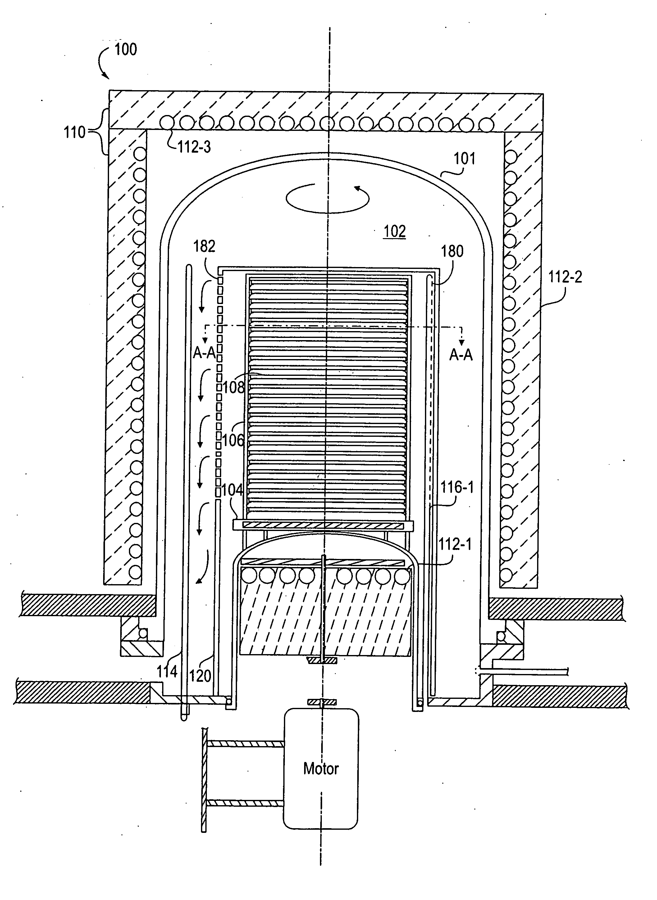
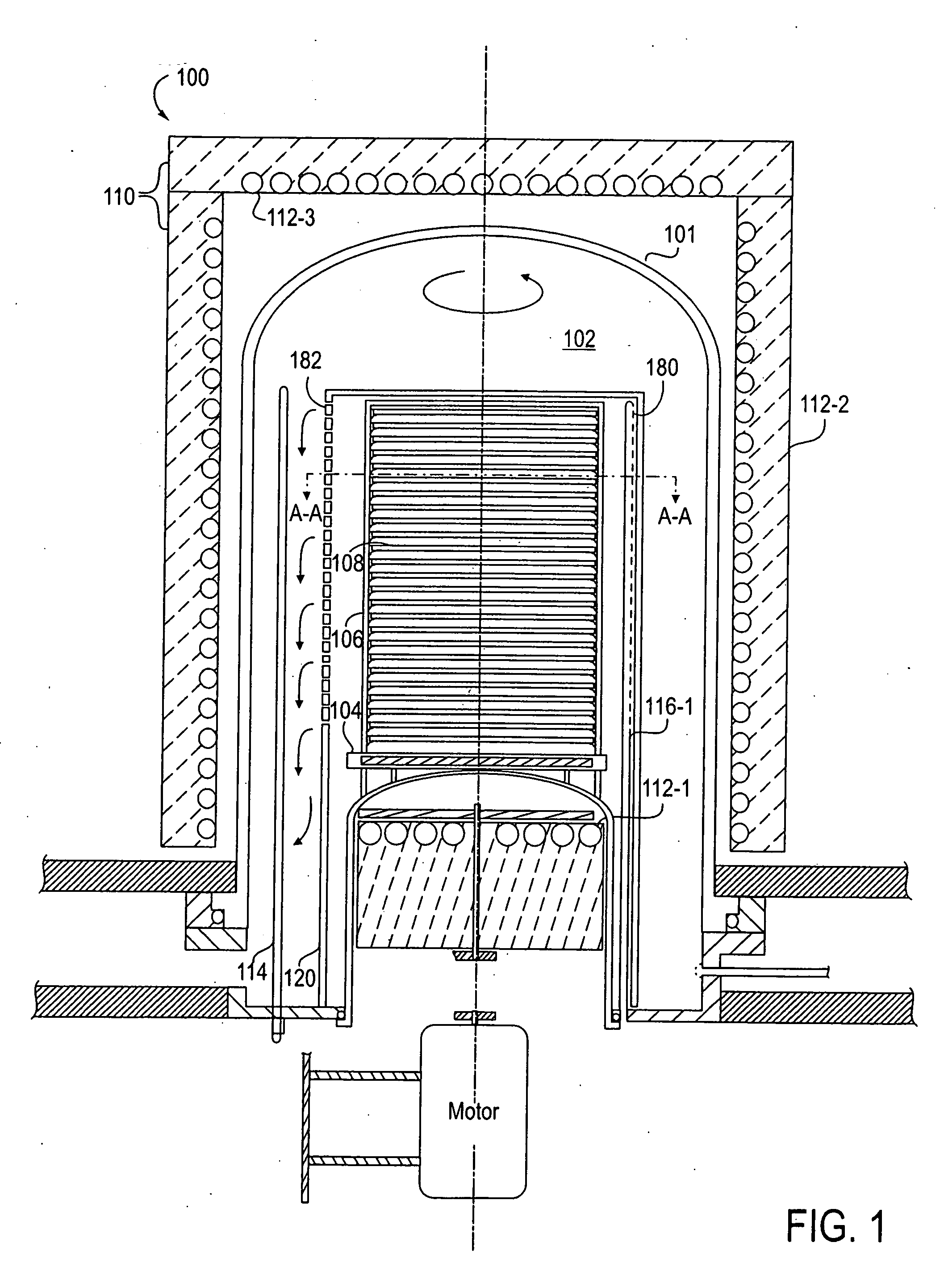
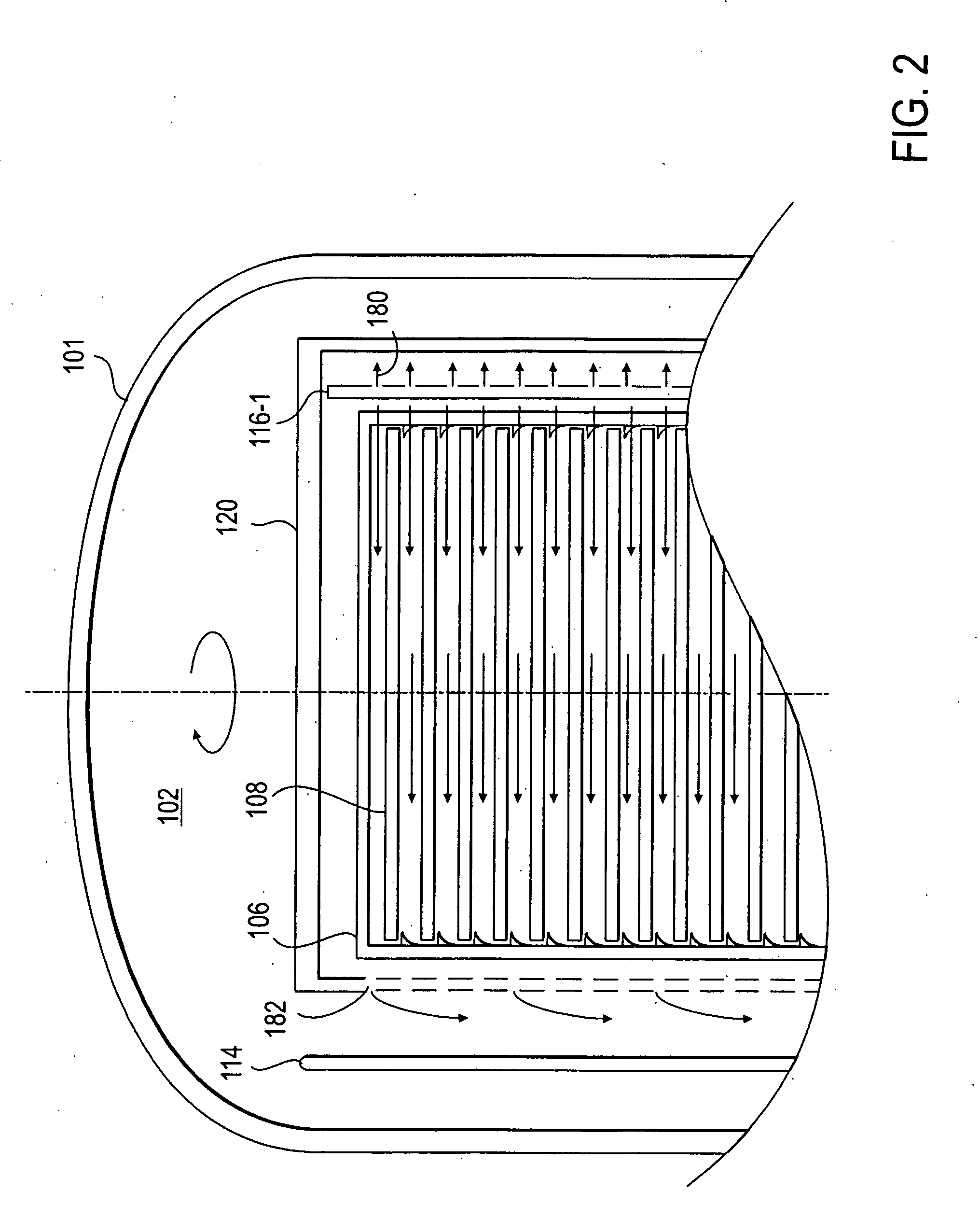
[0018] In general, the inventors have discovered methods that provide for the deposition of silicon containing dielectric materials. The dielectric materials will find uses in the manufacture of semiconductor structures such as spacers, etch stops, hard masks, gates dielectrics, capacitor dielectrics, and the like. In some embodiments the methods provide for the deposition of the dielectric materials using silylamine precursors by chemical vapor deposition (CVD) . In alternative embodiments, atomic layer deposition (ALD) is used. In one embodiment of the present invention, a first class of the silylamines has the general formula:

HmN(SiH3)n

where n is an integer from 1 to 3 and m is equal to 3−n. In another embodiment, silylamine precursors are provided having the general formula:

HmN(Si2H5)n

where n is an integer from 1 to 3 and m is equal to 3−n. In the present invention, the term “silylamine(s)” will be understood to include all members of both classes of these compounds.

[0019...


PUM

PropertyMeasurementUnit
Temperatureaaaaaaaaaa

Abstract

Methods for forming silicon containing films using silylamine moieties are disclosed. In some embodiments, silylamine moieties are employed to deposit silicon-nitrogen, silicon-oxygen, or silicon-nitrogen-oxygen materials at temperatures of less than 550° C. In some embodiments methods are practiced within process chambers adapted to contain a single substrate as well as within process chambers adapted to contain a plurality of substrates, where the silylamine moieties are conveyed to the chambers in across flow type manner.

Description

CROSS REFERENCE TO RELATED APPLICATIONS [0001] This application claims the benefit of, and priority to, of U.S. Provisional Patent Application Ser. No. 60 / 697,763 filed on Jul. 8, 2005, entitled “Method for Depositing Silicon-Containing Films Using ALD” the entire disclosure of which is incorporated herein by reference.FIELD OF THE INVENTION [0002] The present invention relates generally to methods for depositing silicon containing films on the surface of a substrate. Such silicon-containing films comprise silicon-nitrogen, silicon-oxygen, and silicon-nitrogen-oxygen dielectric materials used in the processing of semiconductors. More specifically, embodiments of the present invention provide use of silylamine moieties in the deposition of the silicon containing films carried out at low temperatures, preferably less than approximately 550° C. BACKGROUND OF THE INVENTION [0003] Silicon nitride, silicon dioxide, and silicon oxynitride are dielectric materials widely used in the manufac...

Claims


Application Information

Patent Timeline
IPC IPC(8): C23C16/00
CPCC23C16/308C23C16/345C23C16/401C23C16/402C23C16/4584C23C16/45546C23C16/45553C23C16/45578C23C16/45525C23C16/00
Inventor OKUYAMA, YOSHIKAZUOWYANG, JON S.TREICHEL, HELMUTH
Owner AVIZA TECHNOLOGY INC
Why Eureka
Try Eureka