PCB testing method, PCB manufacturing method and PCB

A technology of printed circuit boards and testing methods, applied in the field of printed circuit boards, can solve problems such as low efficiency, and achieve the effect of improving efficiency and reducing costs

Inactive Publication Date: 2016-08-17
HUAWEI TECH CO LTD
View PDF5 Cites 16 Cited by
  • Summary
  • Abstract
  • Description
  • Claims
  • Application Information

AI Technical Summary

Problems solved by technology

[0006] An embodiment of the present invention provides a method for testing a printed circuit board PCB, a method for manufacturing a PCB, and a PCB, so as to solve the technical problem of low efficiency of methods for detecting line width and line thickness in the prior art

Method used


Image

  • PCB testing method, PCB manufacturing method and PCB
  • PCB testing method, PCB manufacturing method and PCB
  • PCB testing method, PCB manufacturing method and PCB

Examples


Embodiment Construction

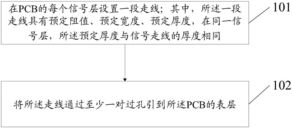
[0034] Embodiments of the present invention provide a method for testing a printed circuit board PCB, a method for manufacturing the PCB, and the PCB, so as to solve the technical problem of low efficiency of methods for detecting line width and line thickness in the prior art.

[0035] The implementation process and purpose of the solution in the embodiment of the present invention will be described in detail below.

[0036] The term "and / or" in this article is just an association relationship describing associated objects, which means that there can be three relationships, for example, A and / or B can mean: A exists alone, A and B exist simultaneously, and there exists alone B these three situations. In addition, the character " / " in this article generally indicates that the contextual objects are an "or" relationship.

[0037] Please refer to as figure 1 As shown, it is a flow chart of the manufacturing method of the PCB in the embodiment of the present invention. Such as...


PUM


Abstract

A PCB testing method, a PCB manufacturing method and the PCB are disclosed. The testing method includes the steps of arranging a section of line on each signal layer of the PCB, leading the section of line to the surface layer of the PCB through at least one pair of through holes, testing the test value of the section of line through the at least one pair of through holes and determining whether the line width and line thickness of signal line of each signal layer meet the standards according to the test value and the preset threshold indicating the preset resistance. The section of line has preset resistance, preset width and preset thickness, the preset thickness is identical to the thickness of the signal lines on a same signal layer, and the length of the line is determined according to the preset resistance, preset width, preset thickness, and the electrical resistivity of the line. The test value indicates the tested resistance of the line.

Description

technical field [0001] The invention relates to the technical field of printed circuit boards, in particular to a method for testing a printed circuit board (PCB), a method for manufacturing the PCB and the PCB. Background technique [0002] The line width and line thickness of a printed circuit board (English: Printed Circuit Board, referred to as: PCB) refer to the width of the traces in each signal layer of the PCB and the thickness of the copper foil. Under normal circumstances, the user will make basic specification requirements for the PCB manufacturer, and the performance indicators of the PCB must meet various design requirements. The PCB manufacturer processes the PCB according to these detailed design requirements, and the user performs acceptance according to this specification, among which line width and line thickness are important acceptance indicators. [0003] Line width and line thickness are the inherent characteristics and important performance indicators...

Claims


Application Information

Patent Timeline
Patent Type & Authority Applications(China)
IPC IPC(8): G01B7/02G01B7/06G01R31/28H05K1/11H05K3/40
CPCG01B7/02G01B7/06G01R31/2813H05K1/11H05K3/40H05K2201/09227
Inventor 张伟朱青松卢艳丽
Owner HUAWEI TECH CO LTD
Why Eureka
Try Eureka