Three-dimensional non-volatile nor-type flash memory

A non-volatile storage and flash memory technology, applied in semiconductor devices, electrical components, circuits, etc., can solve the problems of NAND flash memory that cannot provide random access function storage units and cannot operate independently.

Active Publication Date: 2018-09-21
NOR MEM MICROELECTRONICS CO LTD
View PDF7 Cites 0 Cited by
  • Summary
  • Abstract
  • Description
  • Claims
  • Application Information

AI Technical Summary

Problems solved by technology

However, NAND flash memory cannot provide complete random access function to read each storage unit independently: because the basic storage group of NAND flash memory is formed by connecting some storage units (FETs) in series, the storage unit can only be operated by block when erasing. Operates independently as a single storage unit

Method used


Image

  • Three-dimensional non-volatile nor-type flash memory
  • Three-dimensional non-volatile nor-type flash memory
  • Three-dimensional non-volatile nor-type flash memory

Examples


Embodiment Construction

[0016] The present invention will be further described in detail below in conjunction with the accompanying drawings and embodiments. It should be understood that the specific embodiments described here are only used to explain the present invention, but not to limit the present invention. In addition, it should be noted that, for the convenience of description, only some structures related to the present invention are shown in the drawings but not all structures.

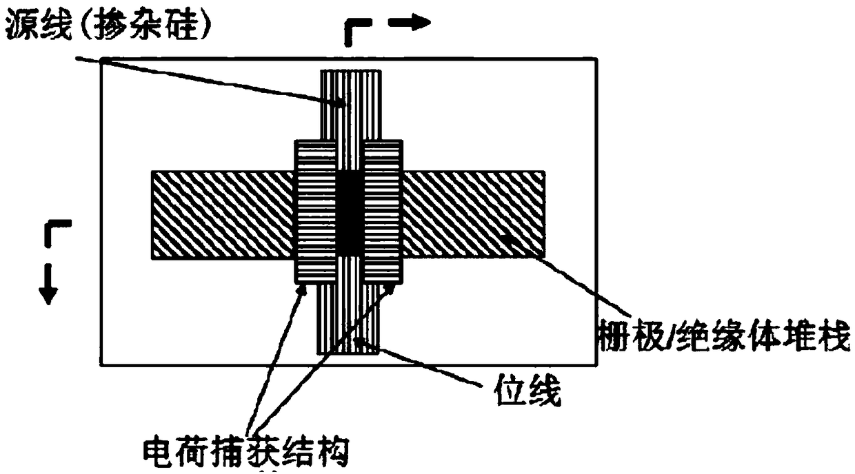
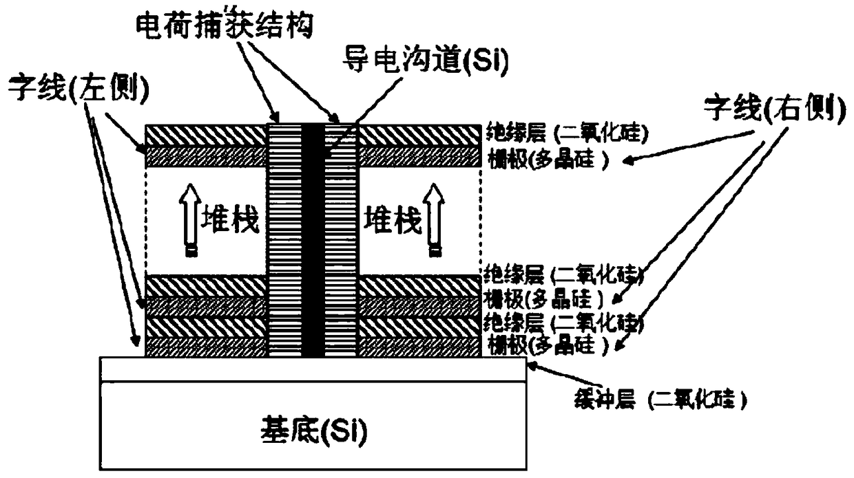
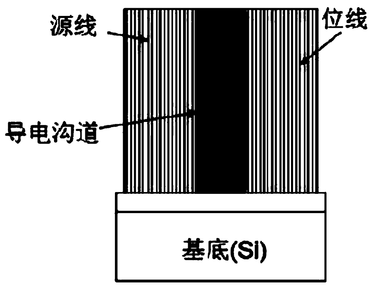
[0017] The invention provides the design of a three-dimensional non-volatile NOR flash memory device that can increase storage density. The main elements include: (1) a basic NOR memory group in which memory cells (i.e., FETs) are stacked in a direction not parallel to the substrate plane and circuits are connected in parallel (i.e., share source and drain) to achieve high storage density; (2 ) basic NOR memory group, wherein each memory cell (i.e. FET) is stacked along the direction parallel to the substrate plan...


PUM


Abstract

The present invention provides some device structures of three-dimensional nonvolatile NOR flash memory: these flash memory devices are formed by connecting a series of basic NOR memory groups provided by the present invention into an array, and each memory cell (field effect transistor) in these basic NOR memory groups Stacking / arranging along a certain direction (perpendicular, oblique, or parallel to the substrate plane direction) and forming a parallel connection on the circuit to achieve high storage density (up to 1Tb level) at low cost. These three-dimensional NOR flash memory devices can not only realize independent complete random access to any single memory cell, but also perform parallel write / erase operations on any number of selected memory cell groups, so they can be widely used in executable code storage and large-capacity data storage applications.

Description

[0001] This application claims the benefit of and priority to the following patent applications: (1) U.S. Provisional Patent Application No. 62 / 097,079 (titled "THREE-DIMENSIONAL NON-VOLATILE NOR-TYPE FLASH MEMORY", filed December 28, 2014) (2) U.S. Patent Application No. 14 / 860,697 (titled "THREE-DIMENSIONAL NON-VOLATILENOR-TYPE FLASH MEMORY", filed September 21, 2015). The contents of the above patent applications are incorporated by reference into this application for all purposes. technical field [0002] The invention relates to a three-dimensional non-volatile NOR flash memory device: it has high storage density and the ability of randomly accessing any single storage unit. Background technique [0003] Flash memory is a widely used non-volatile computer storage technology. It usually uses a floating gate (floating gate) or a charge trap structure (charge trap) to store charges in a field effect transistor (FET) to form a memory unit. According to the difference betwe...

Claims


Application Information

Patent Timeline
Patent Type & Authority Patents(China)
IPC IPC(8): H01L27/11551H01L27/11578
CPCH10B43/00H10B43/20
Inventor 彭海兵
Owner NOR MEM MICROELECTRONICS CO LTD
Why Eureka
Try Eureka