

Method and apparatus for testing transmitter chip
A test method and test device technology, applied in transmitter monitoring, transmission monitoring, electrical components, etc., can solve the problems of increasing test cost, difficulty in improving calibration and test efficiency, and inability to test multiple chips at the same time, so as to achieve saving Cost, the effect of improving test efficiency
Inactive Publication Date: 2016-08-24
BEIJING WINNER MICROELECTRONICS
View PDF10 Cites 7 Cited by
- Summary
- Abstract
- Description
- Claims
- Application Information
AI Technical Summary
Problems solved by technology
This method requires additional instrumentation, increasing the cost of testing
At the same time, one instrument can only correspond to one RF chip. If you do not purchase multiple instruments, it is impossible to test multiple chips at the same time, and it is difficult to improve the efficiency of calibration and testing.
Method used
View moreImage
Smart ImageViewing Examples

Examples
Embodiment 1
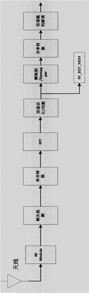
[0040] Based on the requirements of the communication system for cost, area, power consumption and integration, the zero-IF transceiver has a simpler structure, higher bandwidth, smaller area and lower power consumption than the superheterodyne transceiver. It is widely used in communication systems.
Login to View More PUM
 Abstract
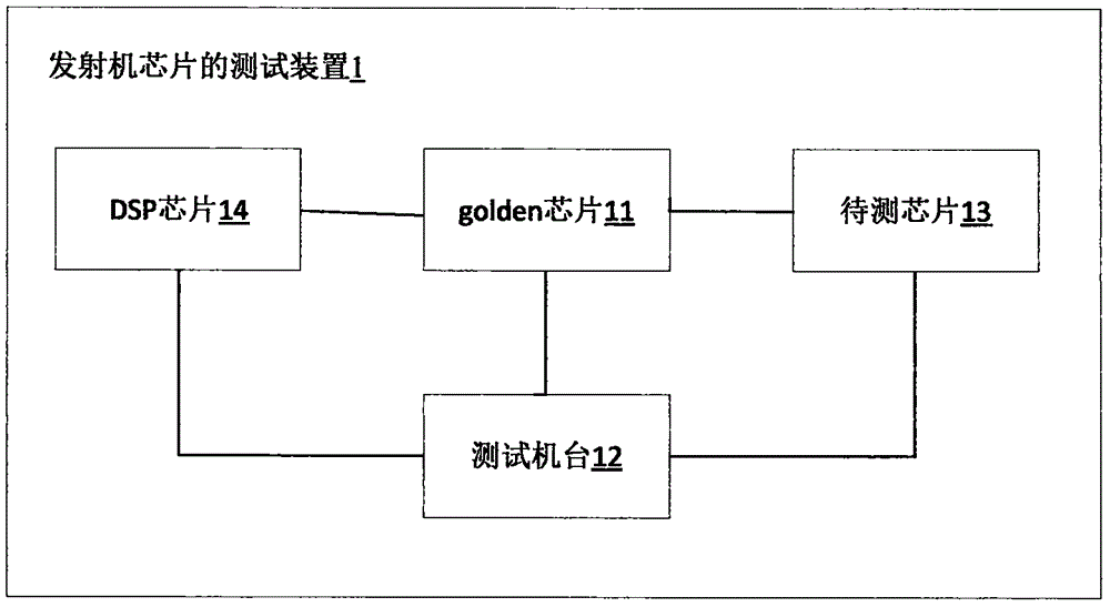
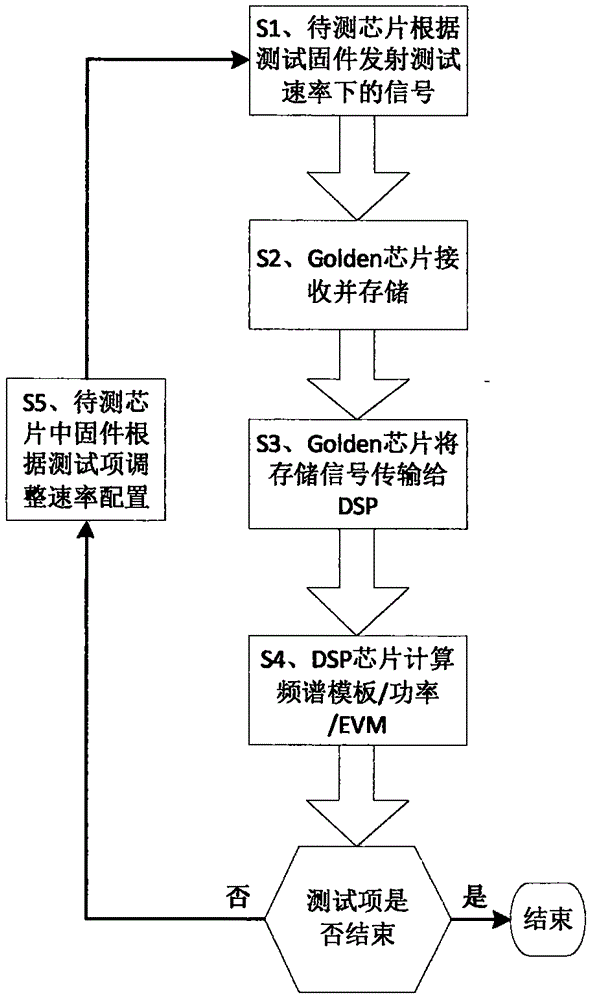
The invention relates to a method and apparatus for testing a transmitter chip. The method comprises the steps: receiving a signal of a chip to be tested according to the transmitted test rate of a test firmware; sending the signal under the test rate to a digital signal processing chip so as to enable the digital signal processing chip to calculate and analyze the signal under the test rate to obtain the test result; and sending the test result to a testing machine. The method and apparatus for testing a transmitter chip utilize the chip to transmit and receive the signal of a chip to be tested and to analyze the signal so as to replace an instrument in a traditional calibration and testing mode, and can realize automatic calibration and testing through the firmware.
Description
technical field [0001] The invention relates to the field of WIFI chips for the Internet of Things, in particular to a testing method and device for a transmitter chip. Background technique [0002] Due to the difference of devices in the chip manufacturing process and the influence of temperature and external environment on the operation of the internal devices of the chip, even the RF chips produced in the same batch will have certain differences in performance. In order to ensure the consistency of the product, before the product is delivered, the analog circuit of the WIFI RF chip will be calibrated with DC bias, in-phase I / quadrature Q two-way phase and amplitude, to correct the analog circuit due to the process deviation in the manufacturing process. The impact of work, and performance testing will also be carried out to ensure that the delivered products meet the performance requirements. [0003] Generally, when calibrating and testing radio frequency chips, specifi...
Claims
Login to View More Application Information
Patent Timeline
 Patent Type & AuthorityApplications(China)
IPC IPC(8): H04B17/10H04B17/15
CPCH04B17/101H04B17/15
Inventor梅张雄程晟
OwnerBEIJING WINNER MICROELECTRONICS