Check patentability & draft patents in minutes with Patsnap Eureka AI!

Circuit board splice board and processing method thereof

A processing method and circuit board technology, applied in the directions of printed circuits, printed circuits, printed circuit components, etc., can solve the impact of the strength and stability of the circuit board assembly, affect the welding effect of electronic components, and the deformation of the circuit board assembly, etc. problems, to achieve the best welding effect, increase the quality of the patch, and prevent bending and deformation.

Active Publication Date: 2016-09-21
GUANGDONG OPPO MOBILE TELECOMM CORP LTD
View PDF8 Cites 2 Cited by
  • Summary
  • Abstract
  • Description
  • Claims
  • Application Information

AI Technical Summary

Problems solved by technology

However, when there is a large opening area on the formed circuit board panel, it will inevitably affect the strength and stability of the entire circuit board panel, resulting in deformation of the circuit board panel
At the same time, due to the existence of the above-mentioned large opening area, the above-mentioned circuit board assembly will affect the soldering effect of electronic components due to uneven heating during the furnace, which will lead to a decrease in the quality of the patch.

Method used


Image

  • Circuit board splice board and processing method thereof
  • Circuit board splice board and processing method thereof
  • Circuit board splice board and processing method thereof

Examples


Embodiment Construction

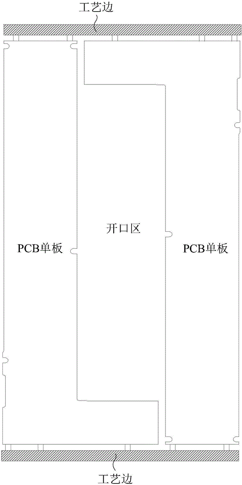
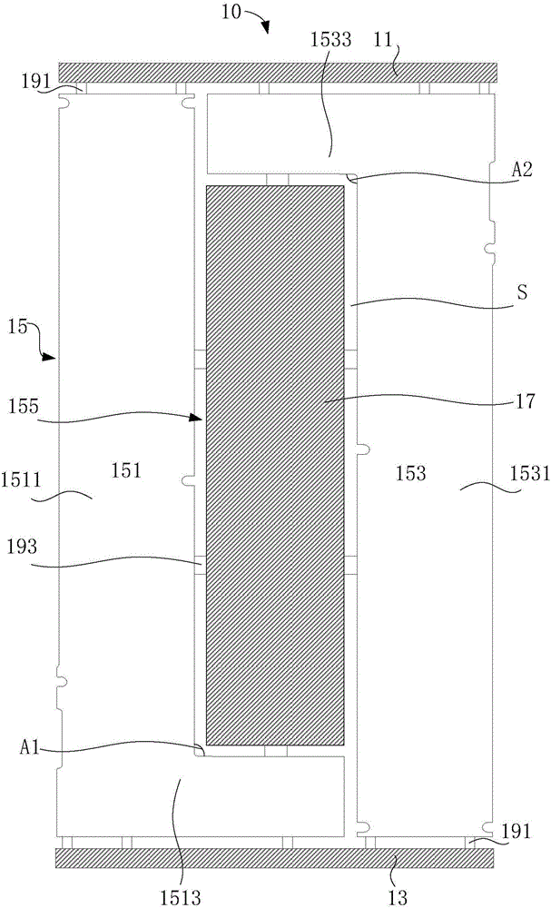
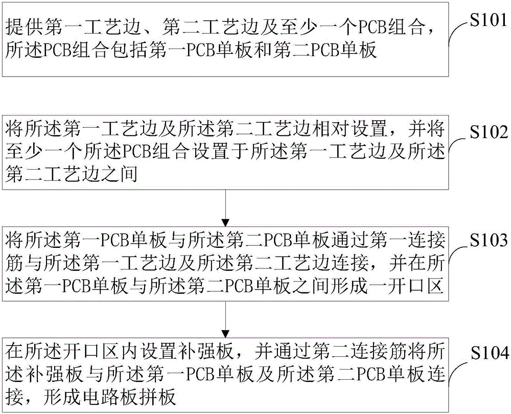
[0028] The following will clearly and completely describe the technical solutions in the embodiments of the present invention with reference to the accompanying drawings in the embodiments of the present invention. Obviously, the described embodiments are only some, not all, embodiments of the present invention. Based on the embodiments of the present invention, all other embodiments obtained by persons of ordinary skill in the art without making creative efforts belong to the protection scope of the present invention.

[0029] For ease of description, spatially relative terms such as "under", "beneath", "below", "above", "on" and other spatially relative terms may be used herein to describe an element as shown in the drawings Or the relationship of a feature to another element or feature(s). It will be understood that when an element or layer is referred to as being "on," "connected to," or "coupled to" another element or layer, it can be directly on, directly on, or directly...


PUM


Abstract

The invention provides a circuit board splice board. The circuit board splice board includes oppositely arranged first technological edge and second technological edge, at least one PCB assembly which is arranged between the first technological edge and the second technological edge, and a reinforcing plate which is connected with the PCB assembly, wherein the PCB assembly includes a first PCB single board and a second PCB single board; the first PCB single board and the second PCB single board are connected with the first technological edge and the second technological edge through first splice bars; an opening area is formed between the first PCB single board and the second PCB single board; and the reinforcing plate is arranged in the opening area, and is connected with the first PCB single board and the second PCB single board through second splice bars. The invention also provides a processing method of the circuit board splice board. The circuit board splice board is higher in the integral intensity and stability.

Description

technical field [0001] The invention relates to the technical field of printed circuit boards, in particular to a circuit board panel and a processing method for the circuit board panel. Background technique [0002] In the printed circuit board (Printed Circuit Board, PCB) manufacturing process, in order to improve the placement efficiency of electronic components such as resistors, capacitors, and inductors, multiple smaller-sized PCB single boards are usually assembled into larger-sized circuit boards. jigsaw puzzle. In the process of forming the circuit board panel, in order to facilitate the molding, the unnecessary waste parts in the circuit board panel will be directly removed. Therefore, in the formed circuit board panel, a gap will be formed on the edge of the PCB veneer, which may resulting in large open areas throughout the board panel, such as figure 1 shown. However, when there is a large opening area on the formed circuit board assembly, it will inevitably a...

Claims


Application Information

Patent Timeline
Patent Type & Authority Applications(China)
IPC IPC(8): H05K1/14H05K3/36
CPCH05K1/14H05K3/36H05K2201/2009
Inventor 黄占肯
Owner GUANGDONG OPPO MOBILE TELECOMM CORP LTD
Features
  • R&D
  • Intellectual Property
  • Life Sciences
  • Materials
  • Tech Scout
  • Unparalleled Data Quality
  • Higher Quality Content
  • 60% Fewer Hallucinations
Learn More