Photosensitive device and its preparation method, photosensitive detector

A technology for photosensitive detectors and photosensitive devices, which is applied in the manufacture of semiconductor devices, electrical components, and final products. The effect of improving detection accuracy and improving photosensitive accuracy

Active Publication Date: 2017-05-17
BOE TECH GRP CO LTD
View PDF4 Cites 0 Cited by
  • Summary
  • Abstract
  • Description
  • Claims
  • Application Information

AI Technical Summary

Problems solved by technology

[0003] However, in practical applications, in order to make the optical signal fully absorbed by the active photosensitive layer 5 without passing through the active photosensitive layer 5, the thickness of the active photosensitive layer 5 is generally set thicker, and since the optical signal is In the active photosensitive layer 5, it is gradually absorbed and converted along its transmission direction, therefore, the light signal close to the metal electrodes 3 and 4 is gradually reduced, thus causing a low concentration of electrons generated near the metal electrodes 3 and 4, such as figure 2 As shown, resulting in a small photosensitive current, and thus the photosensitive accuracy is not high

Method used


Image

  • Photosensitive device and its preparation method, photosensitive detector
  • Photosensitive device and its preparation method, photosensitive detector
  • Photosensitive device and its preparation method, photosensitive detector

Examples


Embodiment 1

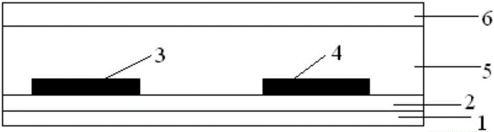
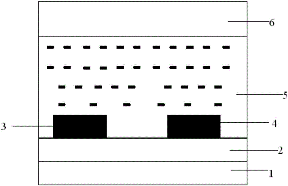
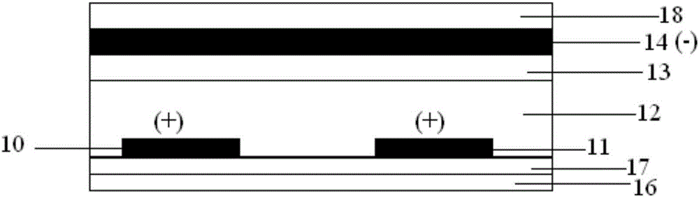
[0028] image 3 A schematic structural diagram of a photosensitive device provided by an embodiment of the present invention; Figure 4 for image 3 Schematic diagram of the electric field within the active photosensitive layer of the photosensitive device shown; see also image 3 with Figure 4 , The photosensitive device provided by the embodiment of the present invention includes: a first electrode 10 , a second electrode 11 , an active photosensitive layer 12 , a first insulating layer 13 and a transparent electrode layer 14 . Wherein, the first insulating layer 13 is formed on the first surface of the active photosensitive layer 12, the active photosensitive layer 12 may be but not limited to GaAs, the first insulating layer 13 may be but not limited to SiN x The transparent electrode layer 14 is formed on the surface of the first insulating layer 13 opposite to the active photosensitive layer 12, the transparent electrode layer 14 can be but not limited to ITO materia...

Embodiment 2

[0042] An embodiment of the present invention provides a photosensitive detector, including a photosensitive device, and the photosensitive device adopts the photosensitive device provided in Embodiment 1 of the present invention.

[0043] The photosensitive detector provided by the present invention can improve detection accuracy because it adopts the above-mentioned photosensitive device provided by the present invention.

Embodiment 3

[0045] Figure 7 For the flow chart of the preparation method of the photosensitive device provided by the embodiment of the present invention, please refer to Figure 7 , the embodiment of the present invention also provides a method for preparing a photosensitive device, comprising the following steps:

[0046] S1, providing an active photosensitive layer, one side of which is formed with a first electrode and a second electrode.

[0047] S2, a first insulating layer is formed on the first surface of the active photosensitive layer, and the first insulating layer is disposed opposite to the first electrode and the second electrode;

[0048] S3, forming a transparent electrode layer on the first insulating layer, where the transparent electrode layer is disposed opposite to the active photosensitive layer;

[0049] S4. Connect both the first electrode and the second electrode to a first power supply, connect the transparent electrode layer to a second power supply, and the ...


PUM


Abstract

The invention provides a photosensitive device and a manufacturing method thereof and a photosensitive detector. The photosensitive device comprises a first electrode, a second electrode, an active photosensitive layer, a first insulating layer and a transparent electrode layer, wherein the first insulating layer is formed on the first surface of the active photosensitive layer; the transparent electrode layer is formed on the surface, opposite to the active photosensitive layer, of the first insulating layer; the first electrode and the second electrode are formed on one side of the second surface, opposite to the first surface, of the active photosensitive layer; the first electrode and the second electrode are connected with a first power supply, the transparent electrode layer is connected with a second power supply, and potential symbols provided by the first power supply and the second power supply are opposite. According to the photosensitive device, the concentration of electrons or holes approaching the first electrode and the second electrode can be improved, so that the photosensitive current can be increased and then the photosensitive precision is improved.

Description

technical field [0001] The invention belongs to the technical field of liquid crystal display, and in particular relates to a photosensitive device, a preparation method thereof, and a photosensitive detector. Background technique [0002] figure 1 For the structural schematic diagram of the photosensitive device of the existing MSM photosensitive detector, please refer to figure 1 , the photosensitive device includes from bottom to top: substrate 1, buffer layer 2, metal electrodes 3 and 4, active photosensitive layer 5, insulating layer 6, the working principle of the photosensitive device is: active photosensitive layer 5 receives photons from the outside And converted into electrons, and then through the voltages loaded on the metal electrodes 3 and 4 respectively, and there is a voltage difference between the two voltages, so that the voltage difference makes the electrons move, thereby forming a current (called photosensitive current), also That is, the optical signa...

Claims


Application Information

Patent Timeline
Patent Type & Authority Patents(China)
IPC IPC(8): H01L31/0224H01L31/18
CPCH01L31/022466H01L31/022475H01L31/18H01L31/1884Y02P70/50
Inventor 马占洁
Owner BOE TECH GRP CO LTD
Why Eureka
Try Eureka